- 您現(xiàn)在的位置:買賣IC網(wǎng) > PDF目錄67320 > 5962-005300HXX (ANALOG DEVICES INC) DUAL 1-CH 12-BIT PROPRIETARY METHOD ADC, PARALLEL ACCESS, CQFP68 PDF資料下載
參數(shù)資料
| 型號(hào): | 5962-005300HXX |
| 廠商: | ANALOG DEVICES INC |
| 元件分類: | ADC |
| 英文描述: | DUAL 1-CH 12-BIT PROPRIETARY METHOD ADC, PARALLEL ACCESS, CQFP68 |
| 封裝: | CERAMIC, LCC-68 |
| 文件頁數(shù): | 3/20頁 |
| 文件大小: | 3346K |
| 代理商: | 5962-005300HXX |
This information applies to a product which is in development. Specifications are subject to change without notice. Contact factory for most
recent information. Analog Devices Sensitive Material - not to be reproduced or distributed without permission.
Rev. Pr E
11
AD13280
JitterConsideration
The signal-to-noise ratio (SNR) for any ADC can be predicted. When
normalized to ADC codes, Equation 1 accurately predicts the SNR
based on three terms. These are jitter, average DNL error, and thermal
noise. Each of these terms contributes to the noise within the converter.
SNR = -20 x log
+ (2 x π x
x tj RMS) 2 +
(1 +
ε)
2N
VNOISE RMS
2N
2
(1)
SNR = -20 x log
+ (2 x π x ANALOG x tj RMS) 2 +
(1 +
ε)
2N
(1 +
ε)
2N
VNOISE RMS
2N
VNOISE RMS
2N
2
(1)
SNR = -20 x log
+ (2 x π x
x tj RMS) 2 +
(1 +
ε)
2N
VNOISE RMS
2N
2
(1)
SNR = -20 x log
+ (2 x π x ANALOG x tj RMS) 2 +
(1 +
ε)
2N
(1 +
ε)
2N
VNOISE RMS
2N
VNOISE RMS
2N
2
(1)
f
ANALOG
= analog input frequency
t
j RMS
= rms jitter of the encode (rms sum of encode
source and internal encode circuitry)
ε
= average DNL of the ADC (typically 0.50 LSB)
N
= Number of bits in the ADC
V
NOISE RMS
= V rms noise referred to the analog
input of the ADC (typically 5 LSB)
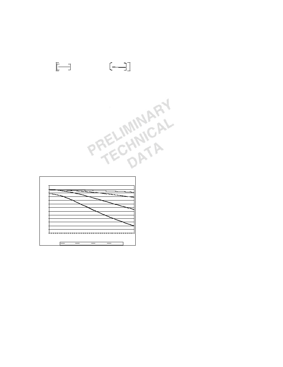
For a 12-bit analog-to-digital converter like the AD13280, aperture jitter
can greatly affect the SNR performance as the analog frequency is
increased. The chart below shows a family of curves that demonstrates
the expected SNR performance of the AD13280 as jitter increases. The
chart is derived from the above equation.
For a complete discussion of aperture jitter, please consult Analog
Devices' Application Note AN-501, "Aperture Uncertainty and ADC
System Performance.
Figure 8. SNR vs Jitter
PowerSupplies
Care should be taken when selecting a power source. Linear supplies
are strongly recommended. Switching supplies tend to have radiated
components that may be "received" by the AD13280. Each of the
power supply pins should be decoupled as closely to the package as
possible using 0.1
F chip capacitors.
The AD13280 has separate digital and analog power supply pins. The
analog supplies are denoted AV
CC
and the digital supply pins are
denoted DV
CC
. AV
CC
and DV
CC
should be separate power supplies.
This is because the fast digital output swings can couple switching
current back into the analog supplies. Note that AV
CC
must be held
within 5% of 5V. The AD13280 is specified for DV
CC
= 3.3V as this is
a common supply for digital ASICs.
Output Loading
Care must be taken when designing the data receivers for the AD13280 .
The digital outputs drive an internal series resistor (e.g. 100
) followed
by a gate like 75LCX574. To minimize capacitive loading, there should
only be one gate on each output pin. An example of this is shown in the
evaluation board schematic shown in Figure. The digital outputs of the
AD13280 have a constant output slew rate of 1 V/ns. A typical CMOS
gate combined with a PCB trace will have a load of approximately
10pF. Therefore, as each bit switches, 10 mA (10 pF X 1 v
÷1ns)of
dynamic current per bit will flow in or out of the device. A full scale
transition can cause up to 140 mA (14 bits X 10 mA/bit) of transient
current through the output stages. These switching currents are
confined between ground and the DV
CC
pin. Standard TTL gates should
be avoided since they can appreciably add to the dynamic switching
currents of the AD13280. It should also be noted that extra capacitive
loading will increase output timing and invalidate timing specifications.
Digital output timing is guaranteed with 10 pF loads.
AD13280 SNR vs. Clock Jitter
58.0
59.0
60.0
61.0
62.0
63.0
64.0
65.0
66.0
67.0
68.0
69.0
70.0
71.0
0.0
0.2
0.4
0.6
0.8
1.0
1.2
1.4
1.6
1.8
2.0
2.2
2.4
2.6
2.8
3.0
3.2
3.4
3.6
3.8
4.0
Clock Jitter (ps)
SNR
(-dBFS)
Ain = 5 MHz
Ain = 10 MHz
Ain = 20 MHz
Ain = 37 MHz
相關(guān)PDF資料 |
PDF描述 |
|---|---|
| 5962-0150601HXX | DUAL 1-CH 14-BIT PROPRIETARY METHOD ADC, PARALLEL ACCESS, CQFP68 |
| 5962-0251002HXC | 1-OUTPUT 8 W DC-DC REG PWR SUPPLY MODULE |
| 5962-9213902HZC | 1-OUTPUT 12 W DC-DC REG PWR SUPPLY MODULE |
| 5962-9555902HXC | 2-OUTPUT 12 W DC-DC REG PWR SUPPLY MODULE |
| 5962-9214402HXC | 2-OUTPUT 15 W DC-DC REG PWR SUPPLY MODULE |
相關(guān)代理商/技術(shù)參數(shù) |
參數(shù)描述 |
|---|---|
| 5962005304899 | 制造商: 功能描述: 制造商:undefined 功能描述: |
| 5962005308115 | 制造商: 功能描述: 制造商:undefined 功能描述: |
| 5962005345643 | 制造商: 功能描述: 制造商:undefined 功能描述: |
| 5962-0053901QYA | 制造商:TI 制造商全稱:Texas Instruments 功能描述:DIGITAL SIGNAL PROCESSOR |
| 5962-0053901QYC | 制造商:TI 制造商全稱:Texas Instruments 功能描述:DIGITAL SIGNAL PROCESSOR |
發(fā)布緊急采購,3分鐘左右您將得到回復(fù)。