- 您現(xiàn)在的位置:買賣IC網(wǎng) > PDF目錄67327 > 5962-8876404XX (ANALOG DEVICES INC) 8-CH 8-BIT FLASH METHOD ADC, PARALLEL ACCESS, CDIP28 PDF資料下載
參數(shù)資料
| 型號(hào): | 5962-8876404XX |
| 廠商: | ANALOG DEVICES INC |
| 元件分類: | ADC |
| 英文描述: | 8-CH 8-BIT FLASH METHOD ADC, PARALLEL ACCESS, CDIP28 |
| 封裝: | 0.600 INCH, GLASS SEALED, CERDIP-28 |
| 文件頁數(shù): | 13/14頁 |
| 文件大小: | 366K |
| 代理商: | 5962-8876404XX |
AD7824/AD7828
REV. D
–8–
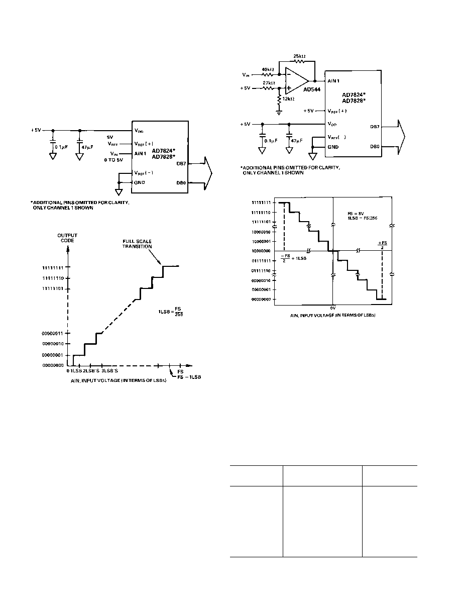
UNIPOLAR OPERATION
The analog input range for any channel of the AD7824/ AD7828
is 0 V to 5 V as shown in the unipolar operational diagram of Fig-
ure 10. Figure 11 shows the designed code transitions which
occur midway between successive integer LSB values (i.e.,
1/2 LSB, 3/2 LSB, 5/2 LSB, FS 3/2 LSBs). The output code is
Natural Binary with 1 LSB = FS/256 = (5/256) V = 19.5 mV.
Figure 10. AD7824/AD7828 Unipolar 0 V to 5 V Operation
Figure 11. Ideal Input/Output Transfer Characteristic for
Unipolar 0 V to 5 V Operation
BIPOLAR OPERATION
The circuit of Figure 12 is designed for bipolar operation. An
AD544 op-amp conditions the signal input (VIN) so that only
positive voltages appear at AIN 1. The closed loop transfer
function of the op amp for the resistor values shown is given
below:
AIN 1 = (2.5 – 0.625
VIN) Volts
The analog input range is
±4 V and the LSB size is 31.25 mV.
The output code is complementary offset binary. The ideal
input/output characteristic is shown in Figure 13.
Figure 12. AD7824/AD7828 Bipolar
±4 V Operation
Figure 13. Ideal Input/Output Transfer Characteristic for
±4 V Operation
TIMING AND CONTROL
The AD7824/AD7828 has two digital inputs for timing and
control. These are Chip Select (
CS) and Read (RD). A READ
operation brings
CS and RD low which starts a conversion on
the channel selected by the multiplexer address inputs (see
Table I). There are two modes of operation as outlined by the
timing diagrams of Figures 14 and 15. Mode 0 is designed for
microprocessors which can be driven into a WAIT state. A
READ operation (i.e.,
CS and RD are taken low) starts a con-
version and data is read when conversion is complete. Mode l
does not require microprocessor WAIT states. A READ operation
initiates a conversion and reads the previous conversion results.
Table I. Truth Table for Input Channel Selection
AD7824
AD7828
A1
A0
A2
A1
A0
Channel
00
0
AIN 1
01
0
1
AIN 2
10
0
1
0
AIN 3
11
0
1
AIN 4
10
0
AIN 5
10
1
AIN 6
11
0
AIN 7
11
1
AIN 8
相關(guān)PDF資料 |
PDF描述 |
|---|---|
| 5962-8876701LA | PARALLEL, WORD INPUT LOADING, 12-BIT DAC, CDIP24 |
| 5962-8877601XX | 1-CH 8-BIT FLASH METHOD ADC, PARALLEL ACCESS, DIP24 |
| 5962-89441012A | SPECIALTY ANALOG CIRCUIT, CQCC20 |
| 5962-8944101VCA | SPECIALTY ANALOG CIRCUIT, CDIP14 |
| 5962-8944101CA | SPECIALTY ANALOG CIRCUIT, CDIP14 |
相關(guān)代理商/技術(shù)參數(shù) |
參數(shù)描述 |
|---|---|
| 5962-8876501RX | 功能描述:數(shù)模轉(zhuǎn)換器- DAC DUAL 12-BIT IC RoHS:否 制造商:Analog Devices 轉(zhuǎn)換器數(shù)量:4 DAC 輸出端數(shù)量:4 轉(zhuǎn)換速率: 分辨率:12 bit 接口類型:Serial (I2C) 穩(wěn)定時(shí)間: 最大工作溫度:+ 105 C 安裝風(fēng)格: 封裝 / 箱體:TSSOP 封裝:Reel |
| 5962-8876502RA | 制造商:Rochester Electronics LLC 功能描述:12-BIT DAC IC - Bulk |
| 5962-8876502RX | 功能描述:數(shù)模轉(zhuǎn)換器- DAC DUAL 12-BIT IC RoHS:否 制造商:Analog Devices 轉(zhuǎn)換器數(shù)量:4 DAC 輸出端數(shù)量:4 轉(zhuǎn)換速率: 分辨率:12 bit 接口類型:Serial (I2C) 穩(wěn)定時(shí)間: 最大工作溫度:+ 105 C 安裝風(fēng)格: 封裝 / 箱體:TSSOP 封裝:Reel |
| 5962-88766013A | 制造商:Analog Devices 功能描述:DAC 1-CH R-2R 12-bit 28-Pin CLLCC 制造商:Analog Devices 功能描述:DAC 1CH R-2R 12-BIT 28CLLCC - Rail/Tube 制造商:Rochester Electronics LLC 功能描述:PARALLEL 12-BIT DACPORT - Bulk 制造商:Analog Devices Inc. 功能描述:Digital to Analog Converters - DAC PARALLEL 12-BIT DACPORT |
| 5962-8876601LA | 功能描述:數(shù)模轉(zhuǎn)換器- DAC 12 BIT V-OUT IC RoHS:否 制造商:Analog Devices 轉(zhuǎn)換器數(shù)量:4 DAC 輸出端數(shù)量:4 轉(zhuǎn)換速率: 分辨率:12 bit 接口類型:Serial (I2C) 穩(wěn)定時(shí)間: 最大工作溫度:+ 105 C 安裝風(fēng)格: 封裝 / 箱體:TSSOP 封裝:Reel |
發(fā)布緊急采購,3分鐘左右您將得到回復(fù)。