- 您現(xiàn)在的位置:買賣IC網(wǎng) > PDF目錄382811 > 71V433S12PFI (Integrated Device Technology, Inc.) 32K x 32 3.3V Synchronous SRAM Flow-Through Outputs PDF資料下載
參數(shù)資料
| 型號: | 71V433S12PFI |
| 廠商: | Integrated Device Technology, Inc. |
| 英文描述: | 32K x 32 3.3V Synchronous SRAM Flow-Through Outputs |
| 中文描述: | 32K的× 32 3.3同步SRAM的流量通過輸出 |
| 文件頁數(shù): | 2/19頁 |
| 文件大小: | 261K |
| 代理商: | 71V433S12PFI |
2
IDT71V433
32K x 32, 3.3V Synchronous SRAM with Flow-Through Outputs Commercial and Industrial Temperature Ranges
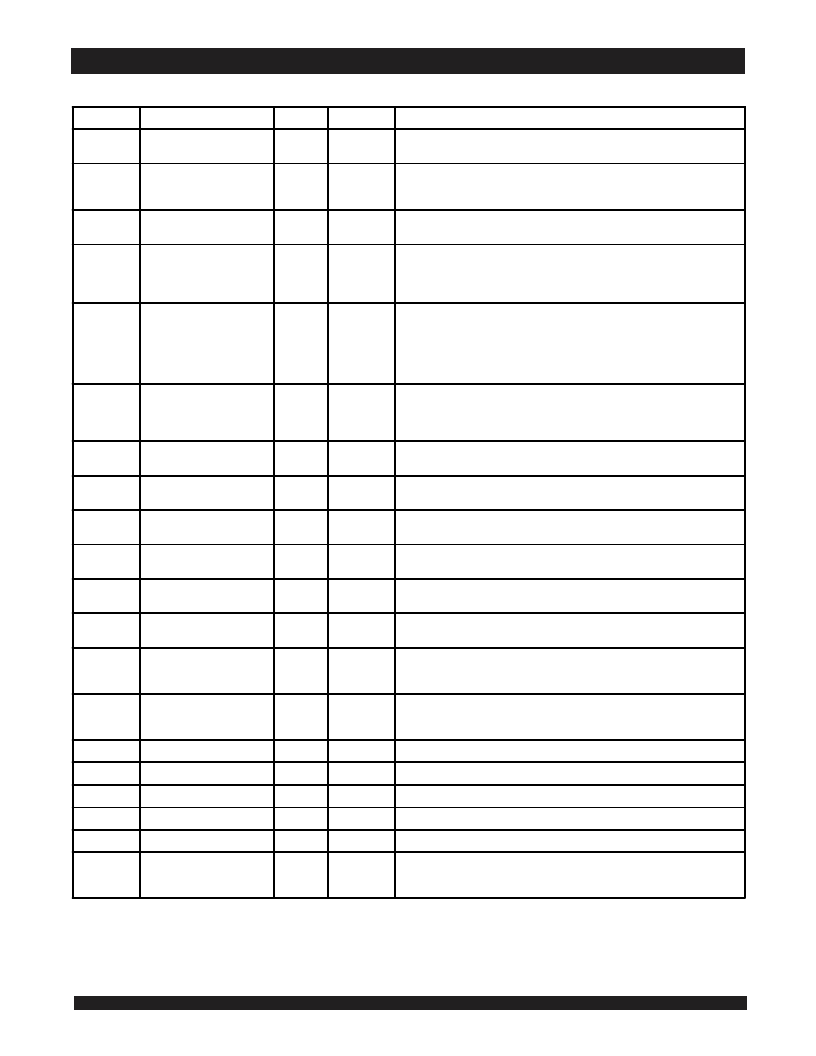
Pin Definitions
(1)
Symbol
Pin Function
I/O
Active
Description
A
0
–A
14
Address Inputs
I
N/A
Synchronous Address inputs. The address register is triggered by a combination
of the rising edge of CLK and
ADSC
Lowor
ADSP
Lowand
CE
Low
ADSC
Address Status
(Cache Controller)
I
LOW
Synchronous Address Status fromCache Controller
ADSC
is an active LOW input
that is used to load the address registers with new addresses.
ADSC
is NOT gated
by
CE
.
ADSP
Address Status (Processor)
I
LOW
Synchronous Address Status fromProcessor
ADSP
is an active LOW input that
is used to load the address registers with new addresses.
ADSP
is gated by
CE
.
ADV
Burst Address Advance
I
LOW
Synchronous Address Advance.
ADV
is an active LOW input that is used to
advance the internal burst counter controlling burst access after the initial address
is loaded. When this input is HIGH the burst counter is not incremented; that is,
there is no address advance.
BWE
Byte Write Enable
I
LOW
Synchronous byte write enable gates the byte write inputs
BW
1
–
BW
4
. If
BWE
is
LOW at the rising edge of CLK then
BW
X
inputs are passed to the next stage in
the circuit. A byte write can still be blocked if
ADSP
is LOW at the rising edge of
CLK. If
ADSP
is HIGH and
BW
X
is LOW at the rising edge of CLK then data will
be written to the SRAM. If
BWE
is HIGH then the byte write inputs are blocked
and only
GW
can initiate a write cycle.
BW
1
–
BW
4
Individual Byte Write
Enables
I
LOW
Synchronous byte write enables.
BW
1
controls I/O(7:0),
BW
controls I/O(15:8),
etc. Any active byte write causes all outputs to be disabled.
ADSP
LOW disables
all byte writes.
BW
1
–
BW
4
must meet specified setup and hold times with respect
to CLK.
CE
Chip Enable
I
LOW
Synchronous chip enable.
CE
is used with CS
0
and
CS
1
to enable the IDT71V433.
CE
also gates
ADSP
.
CLK
Clock
I
N/A
This is the clock input. All timng references for the device are made with respect
to this input.
CS
0
Chip Select 0
I
HIGH
Synchronous active HIGH chip select. CS
0
is used with
CE
and
CS
1
to enable the
chip.
CS
1
Chip Select 1
I
LOW
Synchronous active LOW chip select.
CS
1
is used wth
CE
and CS
0
to enable the
chip.
GW
Global Write Enable
I
LOW
Synchronous global write enable. This input will write all four 8-bit data bytes when
LOW on the rising edge of CLK.
GW
supercedes individual byte write enables.
I/O
0
–I/O
31
Data Input/Output
I/O
N/A
Synchronous data input/output (I/O) pins. Only the data input path is registered
and triggered by the rising edge of CLK. Outputs are Flow-Through.
LBO
Linear Burst
I
LOW
When
LBO
is HIGH the Interleaved Order (Intel) burst sequence is selected. When
LBO
is LOW the Linear (PowerPC) burst sequence is selected.
LBO
has an internal
pull-up resistor
OE
Output Enable
I
LOW
Asynchronous output enable. When
OE
is HIGH the I/O pins are in a high-
impedence state. When
OE
is LOW the data output drivers are enabled if the chip
is also selected.
V
DD
Power Supply
N/A
N/A
3.3V core power supply inputs.
V
DDQ
Power Supply
N/A
N/A
3.3V I/O power supply inputs.
V
SS
Ground
N/A
N/A
Core ground pins.
V
SSQ
Ground
N/A
N/A
I/O ground pins.
NC
No Connect
N/A
N/A
NC pins are not electrically connected to the chip.
ZZ
Sleep Mode
I
HIGH
Asynchronous sleep mode input. ZZ HIGH will gate the CLK internally and power
down the IDT71V433 to its lowest power consumption level. Data retention is
guaranteed in Sleep Mode. ZZ has an internal pull-down resistor
3729 tbl 02
NOTE:
1. All synchronous inputs must meet specified setup and hold times with respect to CLK.
相關(guān)PDF資料 |
PDF描述 |
|---|---|
| 7207 | T-1 Subminiature Lamps |
| 7200 | T-1 Subminiature Lamps |
| 7201 | T-1 Subminiature Lamps |
| 7203 | T-1 Subminiature Lamps |
| 7205 | T-1 Subminiature Lamps |
相關(guān)代理商/技術(shù)參數(shù) |
參數(shù)描述 |
|---|---|
| 71V546S100PF | 制造商:Integrated Device Technology Inc 功能描述:SRAM Chip Sync Single 3.3V 4.5M-Bit 128K x 36 5ns 100-Pin TQFP Tray |
| 71V546S100PF8 | 制造商:Integrated Device Technology Inc 功能描述:SRAM Chip Sync Single 3.3V 4.5M-Bit 128K x 36 5ns 100-Pin TQFP T/R |
| 71V546S100PFG | 功能描述:靜態(tài)隨機存取存儲器 128Kx36 ZBT SYNC 3.3V PIPELINED 靜態(tài)隨機存取存儲器 RoHS:否 制造商:Cypress Semiconductor 存儲容量:16 Mbit 組織:1 M x 16 訪問時間:55 ns 電源電壓-最大:3.6 V 電源電壓-最小:2.2 V 最大工作電流:22 uA 最大工作溫度:+ 85 C 最小工作溫度:- 40 C 安裝風(fēng)格:SMD/SMT 封裝 / 箱體:TSOP-48 封裝:Tray |
| 71V546S100PFG8 | 制造商:Integrated Device Technology Inc 功能描述:SRAM Chip Sync Single 3.3V 4.5M-Bit 128K x 36 5ns 100-Pin TQFP T/R 制造商:Integrated Device Technology Inc 功能描述:SRAM SYNC SGL 3.3V 4.5MBIT 128KX36 5NS 100TQFP - Tape and Reel 制造商:Integrated Device Technology Inc 功能描述:128Kx36 ZBT SYNC 3.3V PIPELINED SRAM |
| 71V546S100PFGI | 功能描述:靜態(tài)隨機存取存儲器 128Kx36 ZBT SYNC 3.3V PIPELINED 靜態(tài)隨機存取存儲器 RoHS:否 制造商:Cypress Semiconductor 存儲容量:16 Mbit 組織:1 M x 16 訪問時間:55 ns 電源電壓-最大:3.6 V 電源電壓-最小:2.2 V 最大工作電流:22 uA 最大工作溫度:+ 85 C 最小工作溫度:- 40 C 安裝風(fēng)格:SMD/SMT 封裝 / 箱體:TSOP-48 封裝:Tray |
發(fā)布緊急采購,3分鐘左右您將得到回復(fù)。