- 您現(xiàn)在的位置:買賣IC網(wǎng) > PDF目錄68812 > 73S1209F-68IMR/F (TERIDIAN SEMICONDUCTOR CORP) POWER SUPPLY MANAGEMENT CKT, QCC68 PDF資料下載
參數(shù)資料
| 型號(hào): | 73S1209F-68IMR/F |
| 廠商: | TERIDIAN SEMICONDUCTOR CORP |
| 元件分類: | 電源管理 |
| 英文描述: | POWER SUPPLY MANAGEMENT CKT, QCC68 |
| 封裝: | LEAD FREE, QFN-68 |
| 文件頁(yè)數(shù): | 93/123頁(yè) |
| 文件大小: | 1385K |
| 代理商: | 73S1209F-68IMR/F |
第1頁(yè)第2頁(yè)第3頁(yè)第4頁(yè)第5頁(yè)第6頁(yè)第7頁(yè)第8頁(yè)第9頁(yè)第10頁(yè)第11頁(yè)第12頁(yè)第13頁(yè)第14頁(yè)第15頁(yè)第16頁(yè)第17頁(yè)第18頁(yè)第19頁(yè)第20頁(yè)第21頁(yè)第22頁(yè)第23頁(yè)第24頁(yè)第25頁(yè)第26頁(yè)第27頁(yè)第28頁(yè)第29頁(yè)第30頁(yè)第31頁(yè)第32頁(yè)第33頁(yè)第34頁(yè)第35頁(yè)第36頁(yè)第37頁(yè)第38頁(yè)第39頁(yè)第40頁(yè)第41頁(yè)第42頁(yè)第43頁(yè)第44頁(yè)第45頁(yè)第46頁(yè)第47頁(yè)第48頁(yè)第49頁(yè)第50頁(yè)第51頁(yè)第52頁(yè)第53頁(yè)第54頁(yè)第55頁(yè)第56頁(yè)第57頁(yè)第58頁(yè)第59頁(yè)第60頁(yè)第61頁(yè)第62頁(yè)第63頁(yè)第64頁(yè)第65頁(yè)第66頁(yè)第67頁(yè)第68頁(yè)第69頁(yè)第70頁(yè)第71頁(yè)第72頁(yè)第73頁(yè)第74頁(yè)第75頁(yè)第76頁(yè)第77頁(yè)第78頁(yè)第79頁(yè)第80頁(yè)第81頁(yè)第82頁(yè)第83頁(yè)第84頁(yè)第85頁(yè)第86頁(yè)第87頁(yè)第88頁(yè)第89頁(yè)第90頁(yè)第91頁(yè)第92頁(yè)當(dāng)前第93頁(yè)第94頁(yè)第95頁(yè)第96頁(yè)第97頁(yè)第98頁(yè)第99頁(yè)第100頁(yè)第101頁(yè)第102頁(yè)第103頁(yè)第104頁(yè)第105頁(yè)第106頁(yè)第107頁(yè)第108頁(yè)第109頁(yè)第110頁(yè)第111頁(yè)第112頁(yè)第113頁(yè)第114頁(yè)第115頁(yè)第116頁(yè)第117頁(yè)第118頁(yè)第119頁(yè)第120頁(yè)第121頁(yè)第122頁(yè)第123頁(yè)

DS_1209F_004
73S1209F Data Sheet
Rev. 1.2
71
1.7.13.2 Answer to Reset Processing
A card insertion event generates an interrupt to the firmware, which is then responsible for the
configuration of the electrical interface, the UART and activation of the card. The activation sequencer
goes through the power up sequence as defined in the ISO 7816-3 specification. An asynchronous
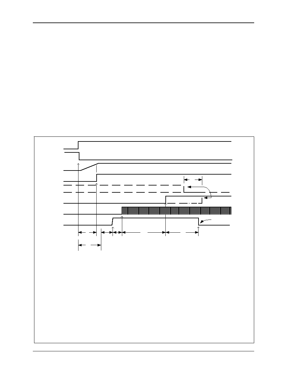
activation timing diagram is shown in Figure 15. After the card reset is de-asserted, the firmware instructs
the hardware to look for a TS byte that begins the ATR response. If a response is not provided within the
pre-programmed timeout period, an interrupt is generated and the firmware can then take appropriate
action, including instructing the 73S1209F to begin a deactivation sequence. Once commanded, the
deactivation sequencer goes through the power down sequence as defined in the ISO 7816-3
specification. If an ATR response is received, the hardware looks for a TS byte that determines
direct/inverse convention. The hardware handles the indirect convention conversion such that the
embedded firmware only receives direct convention. This feature can be disabled by firmware within
SByteCtl register. Parity checking and break generation is performed on the TS byte unless disabled by
firmware. If during the card session, a card removal, over-current or other error event is detected, the
hardware will automatically perform the deactivation sequence and then generate an interrupt to the
firmware. The firmware can then perform any other error handling required for proper system operation.
Smart card RST, I/O and CLK, C4, C8 shall be low before the end of the deactivation sequence. Figure
16 shows the timing for a deactivation sequence.
VCCSEL
bits
VCC
VCCOK bit
RSTCRD bit
RST
CLK
IO
t1
t2
t3
t4
t5
tto
See Note
ATR starts
t4
SELSC
bits
t1: SELSC.1 bit set (selects internal ICC interface) and a non-zero value in VCCSEL bits (calling for a
value of Vcc of 1.8, 3.0, or 5.0 volts) will begin the activation sequence. t1 is the time for Vcc to rise
to acceptable level, declared as Vcc OK (bit VCCOK gets set). This time depends on filter capacitor
value and card Icc load.
tto: The time allowed for Vcc to rise to Vcc OK status after setting of the VCCSEL bits. This time is
generated by the VCCTMR counter. If Vcc OK is not set, (bit VCCOK) at this time, a deactivation will
be initiated. VCCSEL bits are not automatically cleared. The firmware must clear the VCCSEL bits
before starting a new activation.
t2: Time from VCCTmr timeout and VCC OK to IO reception (high), typically 2-3 CLK cycles if
RDYST = 0. If RDYST = 1, t2 starts when VCCOK = 1.
t3: Time from IO = high to CLK start, typically 2-3 CLK cycles.
t4: Time allowed for start of CLK to de-assertion of RST. Programmable by RLength register.
t5: Time allowed for ATR timeout, set by the STSTO register.
Note: If the RSTCRD bit is set, RST is asserted (low). Upon clearing RSTCRD bit, RST will be
de-asserted after t4.
相關(guān)PDF資料 |
PDF描述 |
|---|---|
| 73S1209F-68IM/F | POWER SUPPLY MANAGEMENT CKT, QCC68 |
| 73S1209F-44IMR/F | POWER SUPPLY MANAGEMENT CKT, QCC44 |
| 73S1209F-44IM/F | POWER SUPPLY MANAGEMENT CKT, QCC44 |
| 73S1210F-44IMR/F | 1-CHANNEL POWER SUPPLY MANAGEMENT CKT, QCC44 |
| 73S1210F-68IM/F/P | 1-CHANNEL POWER SUPPLY MANAGEMENT CKT, QCC68 |
相關(guān)代理商/技術(shù)參數(shù) |
參數(shù)描述 |
|---|---|
| 73S1209F-68M/F/P1 | 功能描述:8位微控制器 -MCU Contained 80515-SoC Serial Hst Interface RoHS:否 制造商:Silicon Labs 核心:8051 處理器系列:C8051F39x 數(shù)據(jù)總線寬度:8 bit 最大時(shí)鐘頻率:50 MHz 程序存儲(chǔ)器大小:16 KB 數(shù)據(jù) RAM 大小:1 KB 片上 ADC:Yes 工作電源電壓:1.8 V to 3.6 V 工作溫度范圍:- 40 C to + 105 C 封裝 / 箱體:QFN-20 安裝風(fēng)格:SMD/SMT |
| 73S1209F-EB | 功能描述:開發(fā)板和工具包 - 8051 73S1209F Eval Brd (Doc. Cd, Cable) RoHS:否 制造商:Silicon Labs 產(chǎn)品:Development Kits 工具用于評(píng)估:C8051F960, Si7005 核心: 接口類型:USB 工作電源電壓: |
| 73S1209F-IM44 DK | 制造商:Maxim Integrated Products 功能描述:Development Boards & Kits - 8051 73S1209F Dev Kit Eval Bd Ice Cable Cd |
| 73S1209F-IM44 EB | 制造商:Maxim Integrated Products 功能描述:Development Boards & Kits - 8051 73S1209F Eval Brd Eval Bd Doc Cd Cable |
| 73S1209F-IM68 DK | 制造商:Maxim Integrated Products 功能描述:Development Boards & Kits - 8051 73S1209F Dev Kit Eval Bd Ice Cable Cd |
發(fā)布緊急采購(gòu),3分鐘左右您將得到回復(fù)。