- 您現(xiàn)在的位置:買賣IC網(wǎng) > PDF目錄378210 > 80960CF-40 (Intel Corp.) 32-Bit High-Performance Superscalar Embedded Microprocessor(32位高性能超標(biāo)量嵌入式微處理器) PDF資料下載
參數(shù)資料
| 型號(hào): | 80960CF-40 |
| 廠商: | Intel Corp. |
| 英文描述: | 32-Bit High-Performance Superscalar Embedded Microprocessor(32位高性能超標(biāo)量嵌入式微處理器) |
| 中文描述: | 32位高性能嵌入式微處理器超標(biāo)量(32位高性能超標(biāo)量嵌入式微處理器) |
| 文件頁(yè)數(shù): | 12/77頁(yè) |
| 文件大?。?/td> | 927K |
| 代理商: | 80960CF-40 |
第1頁(yè)第2頁(yè)第3頁(yè)第4頁(yè)第5頁(yè)第6頁(yè)第7頁(yè)第8頁(yè)第9頁(yè)第10頁(yè)第11頁(yè)當(dāng)前第12頁(yè)第13頁(yè)第14頁(yè)第15頁(yè)第16頁(yè)第17頁(yè)第18頁(yè)第19頁(yè)第20頁(yè)第21頁(yè)第22頁(yè)第23頁(yè)第24頁(yè)第25頁(yè)第26頁(yè)第27頁(yè)第28頁(yè)第29頁(yè)第30頁(yè)第31頁(yè)第32頁(yè)第33頁(yè)第34頁(yè)第35頁(yè)第36頁(yè)第37頁(yè)第38頁(yè)第39頁(yè)第40頁(yè)第41頁(yè)第42頁(yè)第43頁(yè)第44頁(yè)第45頁(yè)第46頁(yè)第47頁(yè)第48頁(yè)第49頁(yè)第50頁(yè)第51頁(yè)第52頁(yè)第53頁(yè)第54頁(yè)第55頁(yè)第56頁(yè)第57頁(yè)第58頁(yè)第59頁(yè)第60頁(yè)第61頁(yè)第62頁(yè)第63頁(yè)第64頁(yè)第65頁(yè)第66頁(yè)第67頁(yè)第68頁(yè)第69頁(yè)第70頁(yè)第71頁(yè)第72頁(yè)第73頁(yè)第74頁(yè)第75頁(yè)第76頁(yè)第77頁(yè)
6
PRELIMINARY
80960CF-40, -33, -25, -16
A
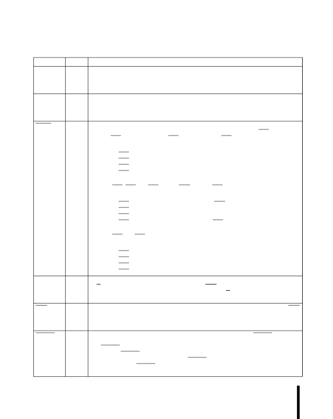
Table 2. 80960CF Pin Description — External Bus Signals
(Sheet 1 of 3)
Name
A31:2
Type
O
S
H(Z)
R(Z)
I/O
S(L)
H(Z)
R(Z)
O
S
H(Z)
R(1)
Description
ADDRESS BUS
carries the physical address’ upper 30 bits. A31 is the most significant
bit; A2 is least significant. During a bus access, A31:2 identify all external addresses to
word (4-byte) boundaries. Byte enable signals indicate the selected byte in each word.
During burst accesses, A3:2 increment to indicate successive data cycles.
DATA BUS
carries 32-, 16- or 8-bit data quantities depending on bus width configura-
tion. The least significant bit is carried on D0 and the most significant on D31. When the
bus is configured for 8-bit data, the lower 8 data lines, D7:0 are used. For 16-bit data
bus widths, D15:0 are used. For 32-bit bus widths the full data bus is used.
BYTE ENABLES
select which of the four bytes addressed by A31:2 are active during
an access to a memory region configured for a 32-bit data-bus width. BE3 applies to
D31:24; BE2 applies to D23:16; BE1 applies to D15:8 BE0 applies to D7:0.
32-bit bus:
BE3
Byte Enable 3
BE2
Byte Enable 2
BE1
Byte Enable 1
BE0
Byte Enable 0
For accesses to a memory region configured for a 16-bit data-bus width, the processor
uses the BE3, BE1 and BE0 pins as BHE, A1 and BLE respectively.
16-bit bus:
BE3
Byte High Enable (BHE)
BE2
Not used (driven high or low)
BE1
Address Bit 1 (A1)
BE0
Byte Low Enable (BLE)
For accesses to a memory region configured for an 8-bit data-bus width, the processor
uses the BE1 and BE0 pins as A1 and A0 respectively.
8-bit bus:
BE3
Not used (driven high or low)
BE2
Not used (driven high or low)
BE1
Address Bit 1 (A1)
BE0
Address Bit 0 (A0)
WRITE/READ
is asserted for read requests and deasserted for write requests. The
W/R signal changes in the same clock cycle as ADS. It remains valid for the entire
access in non-pipelined regions. In pipelined regions, W/R is not guaranteed to be valid
in the last cycle of a read access.
ADDRESS STROBE
indicates a valid address and the start of a new bus access. ADS
is asserted for the first clock of a bus access.
D31:0
BE3:0
enable D31:24
enable D23:16
enable D15:8
enable D7:0
enable D15:8
enable D7:0
W/R
O
S
H(Z)
R(0)
O
S
H(Z)
R(1)
I
S(L)
H(Z)
R(Z)
ADS
READY
READY
is an input which signals the termination of a data transfer. READY is used to
indicate that read data on the bus is valid or that a write-data transfer has completed.
The READY signal works in conjunction with the internally programmed wait-state
generator. If READY is enabled in a region, the pin is sampled after the programmed
number of wait-states has expired. If the READY pin is deasserted, wait states continue
to be inserted until READY becomes asserted. This is true for the N
RAD
, N
RDD
, N
WAD
and N
WDD
wait states. The N
XDA
wait states cannot be extended.
相關(guān)PDF資料 |
PDF描述 |
|---|---|
| 80960CF | 32-Bit High-Performance Superscalar Processor(32位高性能超標(biāo)量處理器) |
| 80960JD | EMBEDDED 32-BIT MICROPROCESSOR |
| 80960JT | EMBEDDED 32-BIT MICROPROCESSOR |
| 80960JF | 3.3 V EMBEDDED 32-BIT MICROPROCESSOR |
| 80960 | 3.3 V EMBEDDED 32-BIT MICROPROCESSOR |
相關(guān)代理商/技術(shù)參數(shù) |
參數(shù)描述 |
|---|---|
| 80960HA | 制造商:INTEL 制造商全稱:Intel Corporation 功能描述:80960HA/HD/HT 32-Bit High-Performance Superscalar Processor |
| 80960HD | 制造商:INTEL 制造商全稱:Intel Corporation 功能描述:80960HA/HD/HT 32-Bit High-Performance Superscalar Processor |
| 80960HT | 制造商:INTEL 制造商全稱:Intel Corporation 功能描述:80960HA/HD/HT 32-Bit High-Performance Superscalar Processor |
| 80960JA | 制造商:INTEL 制造商全稱:Intel Corporation 功能描述:EMBEDDED 32-BIT MICROPROCESSOR |
| 80960JA-25 | 制造商:INTEL 制造商全稱:Intel Corporation 功能描述:EMBEDDED 32-BIT MICROPROCESSOR |
發(fā)布緊急采購(gòu),3分鐘左右您將得到回復(fù)。