- 您現(xiàn)在的位置:買賣IC網(wǎng) > PDF目錄360656 > 9S12B128DGV1 9S12B128 Device Guide PDF資料下載
參數(shù)資料
| 型號: | 9S12B128DGV1 |
| 英文描述: | 9S12B128 Device Guide |
| 中文描述: | 9S12B128設(shè)備指南 |
| 文件頁數(shù): | 81/128頁 |
| 文件大小: | 1823K |
| 代理商: | 9S12B128DGV1 |
第1頁第2頁第3頁第4頁第5頁第6頁第7頁第8頁第9頁第10頁第11頁第12頁第13頁第14頁第15頁第16頁第17頁第18頁第19頁第20頁第21頁第22頁第23頁第24頁第25頁第26頁第27頁第28頁第29頁第30頁第31頁第32頁第33頁第34頁第35頁第36頁第37頁第38頁第39頁第40頁第41頁第42頁第43頁第44頁第45頁第46頁第47頁第48頁第49頁第50頁第51頁第52頁第53頁第54頁第55頁第56頁第57頁第58頁第59頁第60頁第61頁第62頁第63頁第64頁第65頁第66頁第67頁第68頁第69頁第70頁第71頁第72頁第73頁第74頁第75頁第76頁第77頁第78頁第79頁第80頁當(dāng)前第81頁第82頁第83頁第84頁第85頁第86頁第87頁第88頁第89頁第90頁第91頁第92頁第93頁第94頁第95頁第96頁第97頁第98頁第99頁第100頁第101頁第102頁第103頁第104頁第105頁第106頁第107頁第108頁第109頁第110頁第111頁第112頁第113頁第114頁第115頁第116頁第117頁第118頁第119頁第120頁第121頁第122頁第123頁第124頁第125頁第126頁第127頁第128頁
Device User Guide —9S12B128DGV1/D V01.11
81
injectioncurrent mayflowoutofVDD5and couldresult inexternalpowersupply goingoutofregulation.
Ensure external VDD5 load will shunt current greater than maximum injection current. This will be the
greatest risk when the MCU is not consuming power; e.g. if no system clock is present, or if clock rate is
very low which would reduce overall power consumption.
A.1.5 Absolute Maximum Ratings
Absolute maximum ratings are stress ratings only. A functional operation under or outside those maxima
is not guaranteed. Stress beyond those limits may affect the reliability or cause permanent damage of the
device.
This device contains circuitry protecting against damage due to high static voltage or electrical fields;
however, it is advised that normal precautions be taken to avoid application of any voltages higher than
maximum-rated voltages to this high-impedance circuit. Reliability of operation is enhanced if unused
inputs are tied to an appropriate logic voltage level (e.g., either V
SS5
or V
DD5
).
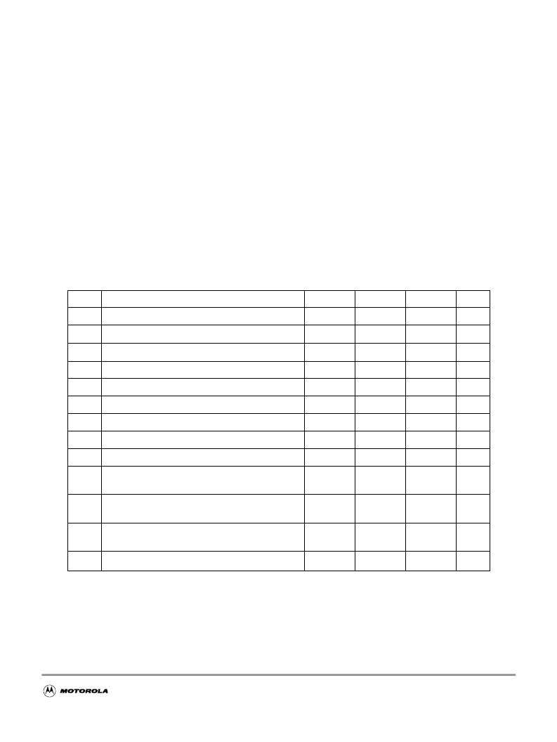
Table A-1 Absolute Maximum Ratings
1
NOTES
:
1. Beyond absolute maximum ratings device might be damaged.
2. The device contains an internal voltage regulator to generate the logic and PLL supply out of the I/O supply.
The absolute maximum ratings apply when the device is powered from an external source.
3. All digital I/O pins are internally clamped to V
SSX
and V
DDX
, V
SSR
and V
DDR
or V
SSA
and V
DDA
.
4. Those pins are internally clamped to V
SSPLL
and V
DDPLL
.
5. This pin is clamped low to V
SSR
, but not clamped high. This pin must be tied low in applications.
Num
Rating
Symbol
Min
Max
Unit
1
I/O, Regulator and Analog Supply Voltage
V
DD5
-0.3
6.5
V
2
Internal Logic Supply Voltage
2
V
DD
-0.3
3.0
V
3
PLL Supply Voltage
2
V
DDPLL
-0.3
3.0
V
4
Voltage difference VDDX to VDDR and VDDA
VDDX
-0.3
0.3
V
5
Voltage difference VSSX to VSSR and VSSA
VSSX
-0.3
0.3
V
6
Digital I/O Input Voltage
V
IN
-0.3
6.5
V
7
Analog Reference
V
RH,
V
RL
-0.3
6.5
V
8
XFC, EXTAL, XTAL inputs
V
ILV
-0.3
3.0
V
9
TEST input
V
TEST
-0.3
10.0
V
10
Instantaneous Maximum Current
Single pin limit for all digital I/O pins
3
I
D
-25
+25
mA
11
Instantaneous Maximum Current
Single pin limit for XFC, EXTAL, XTAL
4
I
DL
-25
+25
mA
12
Instantaneous Maximum Current
Single pin limit for TEST
5
I
DT
-0.25
0
mA
15
Storage Temperature Range
T
stg
– 65
155
°
C
相關(guān)PDF資料 |
PDF描述 |
|---|---|
| 9S12C128DGV1 | MC9S12C Family Device User Guide |
| 9S12D32DGV1 | 9S12DGDJ64DGV1 Device Guide. also covers 9S12D64. 9S12A64. 9S12D32. and 9S12A32 devices |
| 9S12DJ64DGV1 | 9S12DJ64DG Device Guide. also covers 9S12D64. 9S12A64. 9S12D32 and 9S12A32 devices |
| 9S12DJ64-ZIP_PART2 | MC9S12DJ64 Users Guides. zip format. part 2 |
| 9S12DP256BDGV2 | 9S12Dx256B Device Guide. also covers C derivatives and 9S12Ax256 devices |
相關(guān)代理商/技術(shù)參數(shù) |
參數(shù)描述 |
|---|---|
| 9S12C128DGV1 | 制造商:未知廠家 制造商全稱:未知廠家 功能描述:MC9S12C Family Device User Guide |
| 9S12D32DGV1 | 制造商:未知廠家 制造商全稱:未知廠家 功能描述:9S12DGDJ64DGV1 Device Guide. also covers 9S12D64. 9S12A64. 9S12D32. and 9S12A32 devices |
| 9S12DJ64DGV1 | 制造商:未知廠家 制造商全稱:未知廠家 功能描述:9S12DJ64DG Device Guide. also covers 9S12D64. 9S12A64. 9S12D32 and 9S12A32 devices |
| 9S12DP256BDGV1 | 制造商:FREESCALE 制造商全稱:Freescale Semiconductor, Inc 功能描述:Automotive applications |
| 9S12DP256BDGV2 | 制造商:未知廠家 制造商全稱:未知廠家 功能描述:9S12Dx256B Device Guide. also covers C derivatives and 9S12Ax256 devices |
發(fā)布緊急采購,3分鐘左右您將得到回復(fù)。