- 您現(xiàn)在的位置:買賣IC網(wǎng) > PDF目錄352476 > A42MX02-1PQ100B (Electronic Theatre Controls, Inc.) Line Matching Transformer; Current Rating:0A; Insertion Loss:1dB; Leaded Process Compatible:Yes; Peak Reflow Compatible (260 C):Yes; Size:0.89 x 0.812 x 0.715 in; Terminal Type:PCB Thru Hole RoHS Compliant: Yes PDF資料下載
參數(shù)資料
| 型號: | A42MX02-1PQ100B |
| 廠商: | Electronic Theatre Controls, Inc. |
| 英文描述: | Line Matching Transformer; Current Rating:0A; Insertion Loss:1dB; Leaded Process Compatible:Yes; Peak Reflow Compatible (260 C):Yes; Size:0.89 x 0.812 x 0.715 in; Terminal Type:PCB Thru Hole RoHS Compliant: Yes |
| 中文描述: | 40MX和42MX FPGA系列 |
| 文件頁數(shù): | 40/53頁 |
| 文件大小: | 854K |
| 代理商: | A42MX02-1PQ100B |
第1頁第2頁第3頁第4頁第5頁第6頁第7頁第8頁第9頁第10頁第11頁第12頁第13頁第14頁第15頁第16頁第17頁第18頁第19頁第20頁第21頁第22頁第23頁第24頁第25頁第26頁第27頁第28頁第29頁第30頁第31頁第32頁第33頁第34頁第35頁第36頁第37頁第38頁第39頁當(dāng)前第40頁第41頁第42頁第43頁第44頁第45頁第46頁第47頁第48頁第49頁第50頁第51頁第52頁第53頁
40MX and 42MX FPGA Families
v6.0
1-39
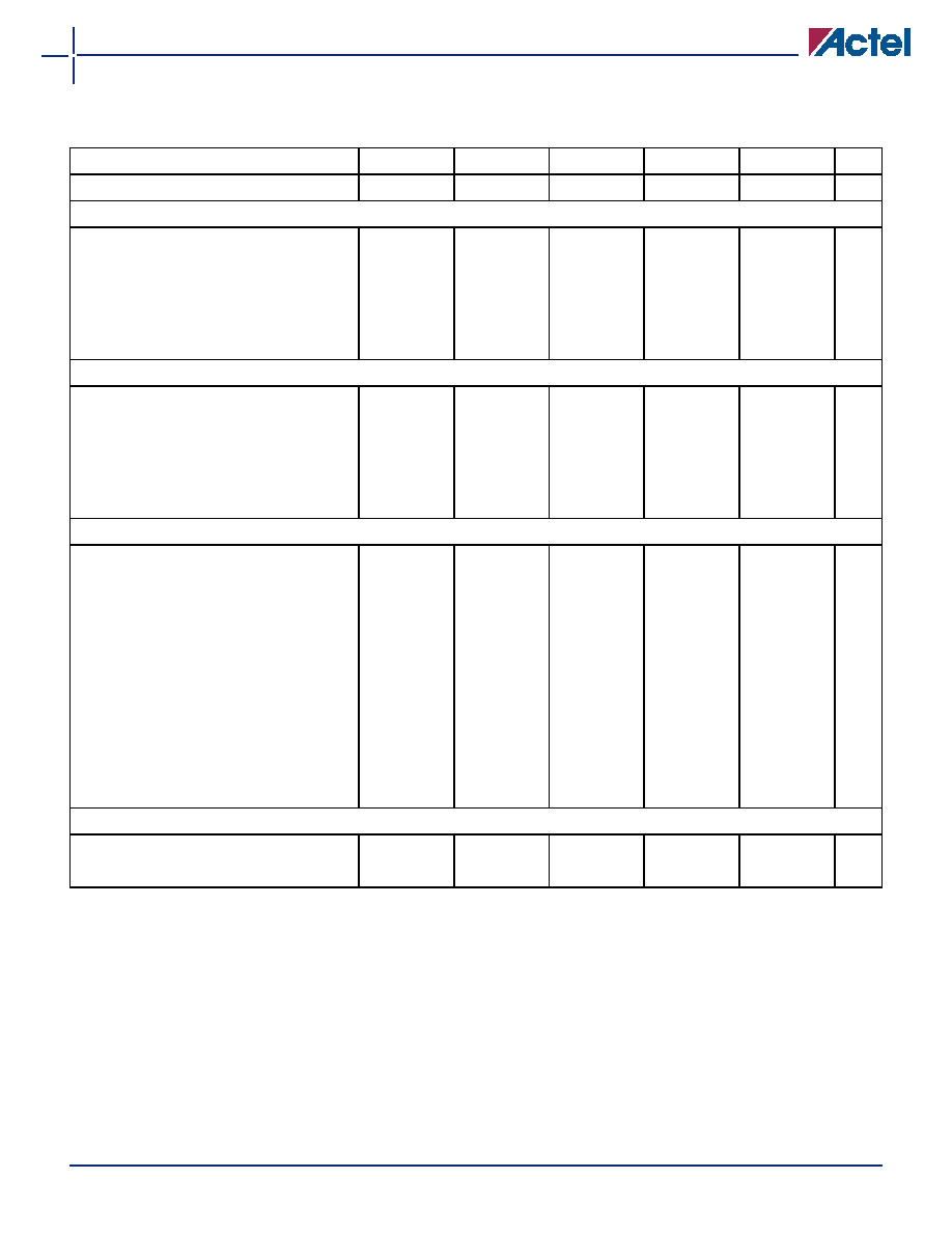
Table 29
A40MX02 Timing Characteristics (Nominal 3.3V Operation)
(Worst-Case Commercial Conditions, VCC = 3.0V, TJ = 70°C)
‘–3’ Speed
‘–2’ Speed
‘–1’ Speed
‘Std’ Speed
‘–F’ Speed
Parameter Description
Min.
Max.
Min.
Max.
Min.
Max.
Min.
Max.
Min.
Max. Units
Logic Module Propagation Delays
tPD1
Single Module
1.7
2.0
2.3
2.7
3.7
ns
tPD2
Dual-Module Macros
3.7
4.3
4.9
5.7
8.0
ns
tCO
Sequential Clock-to-Q
1.7
2.0
2.3
2.7
3.7
ns
tGO
Latch G-to-Q
1.7
2.0
2.3
2.7
3.7
ns
tRS
Flip-Flop (Latch) Reset-to-Q
1.7
2.0
2.3
2.7
3.7
ns
Logic Module Predicted Routing Delays1
tRD1
FO=1 Routing Delay
2.0
2.2
2.5
3.0
4.2
ns
tRD2
FO=2 Routing Delay
2.7
3.1
3.5
4.1
5.7
ns
tRD3
FO=3 Routing Delay
3.4
3.9
4.4
5.2
7.3
ns
tRD4
FO=4 Routing Delay
4.2
4.8
5.4
6.3
8.9
ns
tRD8
FO=8 Routing Delay
7.1
8.2
9.2
10.9
15.2
ns
Logic Module Sequential Timing2
tSUD
Flip-Flop (Latch) Data Input Set-Up
4.3
4.9
5.6
6.6
9.2
ns
tHD
3
Flip-Flop (Latch) Data Input Hold
0.0
ns
tSUENA
Flip-Flop (Latch) Enable Set-Up
4.3
4.9
5.6
6.6
9.2
ns
tHENA
Flip-Flop (Latch) Enable Hold
0.0
ns
tWCLKA
Flip-Flop (Latch) Clock Active
Pulse Width
4.6
5.3
6.0
7.0
9.8
ns
tWASYN
Flip-Flop (Latch)
Asynchronous Pulse Width
4.6
5.3
6.0
7.0
9.8
ns
tA
Flip-Flop Clock Input Period
6.8
7.8
8.9
10.4
14.6
ns
fMAX
Flip-Flop (Latch) Clock
Frequency (FO = 128)
109
101
92
80
48
MHz
Input Module Propagation Delays
tINYH
Pad-to-Y HIGH
1.0
1.1
1.3
1.5
2.1
ns
tINYL
Pad-to-Y LOW
0.9
1.0
1.1
1.3
1.9
ns
Notes:
1. Routing delays are for typical designs across worst-case operating conditions. These parameters should be used for estimating
device performance. Post-route timing analysis or simulation is required to determine actual performance.
2. Set-up times assume fanout of 3. Further testing information can be obtained from the Timer utility.
3. The hold time for the DFME1A macro may be greater than 0 ns. Use the Timer tool from the Designer software to check the hold
time for this macro.
4. Delays based on 35 pF loading.
相關(guān)PDF資料 |
PDF描述 |
|---|---|
| A42MX04-1PQ100B | TRANSF 600 OHM 100MA DC TEL |
| A42MX09-1PQ100B | TRANSF 600 SPLIT PRI .75MA DC TE |
| A42MX16-1PQ100B | TRANSF 600 OHM 0MA DC TEL |
| A42MX24-1PQ100B | TRANSF 600 OHM 0MA DC TEL |
| A42MX02-1PQ100ES | TRANSF 600 OHM 90MA DC TEL |
相關(guān)代理商/技術(shù)參數(shù) |
參數(shù)描述 |
|---|---|
| A42MX02-1PQ100ES | 制造商:未知廠家 制造商全稱:未知廠家 功能描述:40MX and 42MX FPGA Families |
| A42MX02-1PQ100I | 制造商:未知廠家 制造商全稱:未知廠家 功能描述:40MX and 42MX FPGA Families |
| A42MX02-1PQ100M | 制造商:未知廠家 制造商全稱:未知廠家 功能描述:40MX and 42MX FPGA Families |
| A42MX02-1TQ100 | 制造商:未知廠家 制造商全稱:未知廠家 功能描述:40MX and 42MX FPGA Families |
| A42MX02-1TQ100A | 制造商:未知廠家 制造商全稱:未知廠家 功能描述:40MX and 42MX FPGA Families |
發(fā)布緊急采購,3分鐘左右您將得到回復(fù)。