- 您現(xiàn)在的位置:買賣IC網(wǎng) > PDF目錄362029 > A54SX32-2BG329I Field Programmable Gate Array (FPGA) PDF資料下載
參數(shù)資料
| 型號(hào): | A54SX32-2BG329I |
| 英文描述: | Field Programmable Gate Array (FPGA) |
| 中文描述: | 現(xiàn)場(chǎng)可編程門陣列(FPGA) |
| 文件頁(yè)數(shù): | 17/36頁(yè) |
| 文件大小: | 833K |
| 代理商: | A54SX32-2BG329I |
第1頁(yè)第2頁(yè)第3頁(yè)第4頁(yè)第5頁(yè)第6頁(yè)第7頁(yè)第8頁(yè)第9頁(yè)第10頁(yè)第11頁(yè)第12頁(yè)第13頁(yè)第14頁(yè)第15頁(yè)第16頁(yè)當(dāng)前第17頁(yè)第18頁(yè)第19頁(yè)第20頁(yè)第21頁(yè)第22頁(yè)第23頁(yè)第24頁(yè)第25頁(yè)第26頁(yè)第27頁(yè)第28頁(yè)第29頁(yè)第30頁(yè)第31頁(yè)第32頁(yè)第33頁(yè)第34頁(yè)第35頁(yè)第36頁(yè)
v2.0
17
54SX Family FPGAs RadTolerant and HiRel
Timing Characteristics
Timing characteristics for 54SX devices fall into three
categories: family-dependent, device-dependent, and
design-dependent.
The
input
characteristics are common to all 54SX family members.
Internal routing delays are device dependent. Design
dependency means actual delays are not determined until
after placement and routing of the user
’
s design is
complete. Delay values may then be determined by using
the DirectTime Analyzer utility or performing simulation
with post-layout delays.
and
output
buffer
Critical Nets and Typical Nets
Propagation delays are expressed only for typical nets,
which are used for initial design performance evaluation.
Critical net delays can then be applied to the most
time-critical paths. Critical nets are determined by net
property assignment prior to placement and routing. Up to
6 percent of the nets in a design may be designated as
critical, while 90 percent of the nets in a design are typical.
Long Tracks
Some nets in the design use long tracks. Long tracks are
special routing resources that span multiple rows, columns,
or modules. Long tracks employ three and sometimes five
antifuse connections. This increases capacitance and
resistance, resulting in longer net delays for macros
connected to long tracks. Typically up to 6% of nets in a fully
utilized device require long tracks. Long tracks contribute
approximately 4 ns to 8.4 ns delay. This additional delay is
represented statistically in higher fanout (FO=24) routing
delays in the data sheet specifications section.
Timing Derating
54SX devices are manufactured in a CMOS process.
Therefore, device performance varies according to
temperature, voltage, and process variations. Minimum
timing parameters reflect maximum operating voltage,
minimum operating temperature, and best-case processing.
Maximum timing parameters reflect minimum operating
voltage, maximum operating temperature, and worst-case
processing.
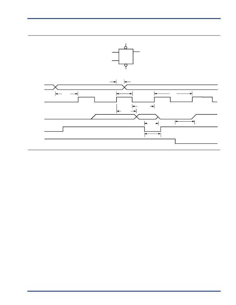
Register Cell Timing Characteristics
Flip-Flops
(Positive edge triggered)
D
CLK
CLR
Q
D
CLK
Q
CLR
t
HPWH
,
t
RPWH
t
WASYN
t
HD
t
SUD
t
HP
t
HPWL
,
t
RPWL
t
RCO
t
CLR
PRESET
t
PRESET
PRESET
相關(guān)PDF資料 |
PDF描述 |
|---|---|
| A54SX32-2TQ144 | Field Programmable Gate Array (FPGA) |
| A54SX32-2TQ144I | Field Programmable Gate Array (FPGA) |
| A54SX08-1FG144 | Field Programmable Gate Array (FPGA) |
| A54SX08-1FG144I | Field Programmable Gate Array (FPGA) |
| A54SX08-1PL84 | Field Programmable Gate Array (FPGA) |
相關(guān)代理商/技術(shù)參數(shù) |
參數(shù)描述 |
|---|---|
| A54SX32-2BG329IX3 | 制造商:Microsemi Corporation 功能描述:FPGA SX Family 32K Gates 1800 Cells 320MHz 0.35um Technology 3.3V/5V 329-Pin BGA 制造商:Microsemi Corporation 功能描述:54SX 32K GATES 1800 MC 320MHZ IND CMOS 3.3/5V 329 BGA - Trays |
| A54SX32-2BGG329 | 功能描述:IC FPGA SX 48K GATES 329-BGA RoHS:是 類別:集成電路 (IC) >> 嵌入式 - FPGA(現(xiàn)場(chǎng)可編程門陣列) 系列:SX 產(chǎn)品培訓(xùn)模塊:Three Reasons to Use FPGA's in Industrial Designs Cyclone IV FPGA Family Overview 特色產(chǎn)品:Cyclone? IV FPGAs 標(biāo)準(zhǔn)包裝:60 系列:CYCLONE® IV GX LAB/CLB數(shù):9360 邏輯元件/單元數(shù):149760 RAM 位總計(jì):6635520 輸入/輸出數(shù):270 門數(shù):- 電源電壓:1.16 V ~ 1.24 V 安裝類型:表面貼裝 工作溫度:0°C ~ 85°C 封裝/外殼:484-BGA 供應(yīng)商設(shè)備封裝:484-FBGA(23x23) |
| A54SX32-2BGG329I | 功能描述:IC FPGA SX 48K GATES 329-BGA RoHS:是 類別:集成電路 (IC) >> 嵌入式 - FPGA(現(xiàn)場(chǎng)可編程門陣列) 系列:SX 產(chǎn)品培訓(xùn)模塊:Three Reasons to Use FPGA's in Industrial Designs Cyclone IV FPGA Family Overview 特色產(chǎn)品:Cyclone? IV FPGAs 標(biāo)準(zhǔn)包裝:60 系列:CYCLONE® IV GX LAB/CLB數(shù):9360 邏輯元件/單元數(shù):149760 RAM 位總計(jì):6635520 輸入/輸出數(shù):270 門數(shù):- 電源電壓:1.16 V ~ 1.24 V 安裝類型:表面貼裝 工作溫度:0°C ~ 85°C 封裝/外殼:484-BGA 供應(yīng)商設(shè)備封裝:484-FBGA(23x23) |
| A54SX322PQ208 | 制造商:ACTEL 功能描述:New |
| A54SX32-2PQ208 | 功能描述:IC FPGA SX 48K GATES 208-PQFP RoHS:否 類別:集成電路 (IC) >> 嵌入式 - FPGA(現(xiàn)場(chǎng)可編程門陣列) 系列:SX 產(chǎn)品培訓(xùn)模塊:Three Reasons to Use FPGA's in Industrial Designs Cyclone IV FPGA Family Overview 特色產(chǎn)品:Cyclone? IV FPGAs 標(biāo)準(zhǔn)包裝:60 系列:CYCLONE® IV GX LAB/CLB數(shù):9360 邏輯元件/單元數(shù):149760 RAM 位總計(jì):6635520 輸入/輸出數(shù):270 門數(shù):- 電源電壓:1.16 V ~ 1.24 V 安裝類型:表面貼裝 工作溫度:0°C ~ 85°C 封裝/外殼:484-BGA 供應(yīng)商設(shè)備封裝:484-FBGA(23x23) |
發(fā)布緊急采購(gòu),3分鐘左右您將得到回復(fù)。