- 您現(xiàn)在的位置:買賣IC網(wǎng) > PDF目錄373891 > AD6640AST (ANALOG DEVICES INC) 12-Bit, 65 MSPS IF Sampling A/D Converter PDF資料下載
參數(shù)資料
| 型號: | AD6640AST |
| 廠商: | ANALOG DEVICES INC |
| 元件分類: | ADC |
| 英文描述: | 12-Bit, 65 MSPS IF Sampling A/D Converter |
| 中文描述: | 1-CH 12-BIT PROPRIETARY METHOD ADC, PARALLEL ACCESS, PQFP44 |
| 封裝: | PLASTIC, MS-026BCB, LQFP-44 |
| 文件頁數(shù): | 21/24頁 |
| 文件大?。?/td> | 488K |
| 代理商: | AD6640AST |
AD6640
REV. 0
–21–
T he simplest method for generating dither is through the use of
a noise diode (Figure 48). In this circuit, the noise diode NC202
generates the reference noise that is gained up and driven by the
AD600 and OP27 amplifier chain. T he level of noise may be
controlled by either presetting the control voltage when the
system is set up, or by using a digital-to-analog converter (DAC)
to adjust the noise level based on input signal conditions. Once
generated, the signal must be introduced to the receiver strip.
T he easiest method is to inject the signal into the drive chain
after the last down conversion as shown in Figure 49.
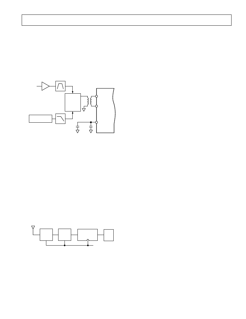
NOISE SOURCE
(REF. FIGURE 48)
LPF
AIN
0.01
m
F
AIN
V
REF
0.1
m
F
AD6640
COMBINER
BPF
FROM
RF/IF
IF AMP
Figure 49. Using the AD6640 with Dither
Receiver E xample
T o determine how the ADC performance relates to overall re-
ceiver sensitivity, the simple receiver in Figure 50 will be exam-
ined. T his example assumes that the overall down conversion
process can be grouped into one set of specifications, instead of
individually examining all components within the system and
summing them together. Although a more detailed analysis
should be employed in a real design, this model will provide a
good approximation.
In examining a wideband digital receiver, several considerations
must be applied. Although other specifications are important,
receiver sensitivity determines the absolute limits of a radio
excluding the effects of other outside influences. Assuming that
receiver sensitivity is limited by noise and not adjacent signal
strength, several sources of noise can be identified and their
overall contribution to receiver sensitivity calculated.
RF/IF
AD6640
ENC
CHANNELIZER
REF IN
DSP
61.44MHz
GAIN = 30dB
NF = 10dB
BW =12.5MHz
SINGLE CHANNEL
BW = 30kHz
Figure 50. Receiver Analysis
T he first noise calculation to make is based on the signal band-
width at the antenna. In a typical broadband cellular receiver,
the IF bandwidth is 12.5 MHz. Given that the power of noise in
a given bandwidth is defined by
P
n
= kTB
, where
B
is band-
width,
k
= 1.38
×
10
–23
is Boltzman’s constant and
T
= 300
k
is absolute temperature, this gives an input noise power of
5.18
×
10
–14
watts or –102.86 dBm. If our receiver front end has
a gain of 30 dB and a noise figure of 10 dB, then the total noise
presented to the ADC input becomes –62.86dBm (–102.86 + 30
+ 10) or 0.16 mV rms. Comparing receiver noise to dither re-
quired for good SFDR, we see that in this example, our receiver
supplies about 3% of the dither required for good SFDR.
Based on a typical ADC SNR specification of 68 dB, the
equivalent internal converter noise is 0.140 mV rms. T here-
fore total broadband noise is 0.21 mV rms. Before process-
ing gain, this is an equivalent SNR (with respect to full scale)
of 64.5 dB. Assuming a 30 kHz AMPS signal and a sample
rate of 61.44 MSPS, the SNR through processing gain is in-
creased by approximately 33 dB to 97.5 dB. However, if eight
strong and equal signals are present in the ADC bandwidth,
then each must be placed 18 dB below full scale to prevent
ADC overdrive. T herefore we give away 18 dB of range and
reduce the carrier-to-noise ratio (C/N) to 79.5 dB.
Assuming that the C/N ratio must be 10 dB or better for
accurate demodulation, one of the eight signals may be reduced by
66.5 dB before demodulation becomes unreliable. At this point,
the input signal power would be –90.5 dBm. Referenced to the
antenna, this is –120.5 dBm.
T o improve sensitivity, several things can be done. First, the
noise figure of the receiver can be reduced. Since front end
noise dominates the 0.16 mV rms, each dB reduction in noise
figure translates to an additional dB of sensitivity. Second, pro-
viding broadband AGC can improve sensitivity by the range of
the AGC. However, the AGC would only provide useful im-
provements if all in-band signals are kept to an absolute minimal
power level so that AGC can be kept near the maximum gain.
T his noise limited example does not adequately demonstrate the
true limitations in a wideband receiver. Other limitations such
as SFDR are more restrictive than SNR and noise. Assume that
the analog-to-digital converter has an SFDR specification of
–80 dBFS or –76 dBm (Full scale = +4 dBm). Also assume
that a tolerable carrier-to-interferer (C/I) (different from C/N)
ratio is 18 dB. T his means that the minimum signal level is
–62 dBFS (–80 plus 18) or –58 dBm. At the antenna, this is
–88 dBm. T herefore, as can be seen, SFDR (single or multi-
tone) would limit receiver performance in this example. How-
ever, as shown previously, SFDR can be greatly improved
through the use of dither (Figures 19, 22). In many cases, the
addition of the out-of-band dither can improve receiver sensitiv-
ity nearly to that limited by thermal noise.
相關(guān)PDF資料 |
PDF描述 |
|---|---|
| AD6640PCB | 12-Bit, 65 MSPS IF Sampling A/D Converter |
| AD6640ST | 12-Bit, 65 MSPS IF Sampling A/D Converter |
| AD6644 | 14-Bit, 40 MSPS/65 MSPS A/D Converter |
| AD6644PCB | 14-Bit, 40 MSPS/65 MSPS A/D Converter |
| AD6644ST | 14-Bit, 40 MSPS/65 MSPS A/D Converter |
相關(guān)代理商/技術(shù)參數(shù) |
參數(shù)描述 |
|---|---|
| AD6640ASTZ | 功能描述:IC ADC 12BIT 65MSPS 44-LQFP RoHS:是 類別:RF/IF 和 RFID >> RF 其它 IC 和模塊 系列:- 標(biāo)準(zhǔn)包裝:100 系列:* |
| AD6640PCB | 制造商:AD 制造商全稱:Analog Devices 功能描述:12-Bit, 65 MSPS IF Sampling A/D Converter |
| AD6640ST | 制造商:AD 制造商全稱:Analog Devices 功能描述:12-Bit, 65 MSPS IF Sampling A/D Converter |
| AD6640ST/PCB | 制造商:Analog Devices 功能描述: |
| AD6641 | 制造商:AD 制造商全稱:Analog Devices 功能描述:250 MHz Bandwidth DPD Observation Receiver |
發(fā)布緊急采購,3分鐘左右您將得到回復(fù)。