- 您現(xiàn)在的位置:買賣IC網(wǎng) > PDF目錄373975 > ADAU1401YSTZ (ANALOG DEVICES INC) SigmaDSP 28-/56-Bit Audio Processor with Two ADCs and Four DACs PDF資料下載
參數(shù)資料
| 型號: | ADAU1401YSTZ |
| 廠商: | ANALOG DEVICES INC |
| 元件分類: | 消費家電 |
| 英文描述: | SigmaDSP 28-/56-Bit Audio Processor with Two ADCs and Four DACs |
| 中文描述: | SPECIALTY CONSUMER CIRCUIT, PQFP48 |
| 封裝: | ROHS COMPLIANT, PLASTIC, MS-026BBC, LQFP-48 |
| 文件頁數(shù): | 19/52頁 |
| 文件大?。?/td> | 785K |
| 代理商: | ADAU1401YSTZ |
第1頁第2頁第3頁第4頁第5頁第6頁第7頁第8頁第9頁第10頁第11頁第12頁第13頁第14頁第15頁第16頁第17頁第18頁當(dāng)前第19頁第20頁第21頁第22頁第23頁第24頁第25頁第26頁第27頁第28頁第29頁第30頁第31頁第32頁第33頁第34頁第35頁第36頁第37頁第38頁第39頁第40頁第41頁第42頁第43頁第44頁第45頁第46頁第47頁第48頁第49頁第50頁第51頁第52頁
ADAU1401
AUDIO ADCs
The ADAU1401 has two Σ-Δ ADCs. The signal-to-noise ratio
(SNR) of the ADCs is 100 dB, and the THD + N is 83 dB.
The stereo audio ADCs are current input; therefore, a voltage-
to-current resistor is required on the inputs. This means that
the voltage level of the input signals to the system can be set to
any level; only the input resistors need to be scaled to provide
the proper full-scale current input. The ADC0 and ADC1 input
pins, as well as ADC_RES, have an internal 2 kΩ resistor for
ESD protection. The voltage seen directly on the ADC input
pins is the 1.5 V common mode.
The external resistor connected to ADC_RES sets the full-scale
current input of the ADCs. The full range of the ADC inputs is
100 μA
rms
with an external 18 kΩ resistor on ADC_RES (20 kΩ
total, because it is in series with the internal 2 kΩ). The only
reason to change the ADC_RES resistor is if a sampling rate
other than 48 kHz is used.
The voltage-to-current resistors connected to ADC0/ADC1 set
the full-scale voltage input of the ADCs. With a full-scale current
input of 100 μA
rms,
a 2.0 V
rms
signal with an external 18 kΩ resistor
(in series with the 2 kΩ internal resistor) results in an input using
the full range of the ADC. The matching of these resistors to the
ADC_RES resistor is important to the operation of the ADCs.
For these three resistors, a 1% tolerance is recommended.
Either the ADC0 and/or ADC1 input pins can be left
unconnected if that channel of the ADC is unused.
These calculations of resistor values assume a 48 kHz sample
rate. The recommended input and current setting resistors
scale linearly with the sample rate because the ADCs have a
switched-capacitor input. The total value (2 kΩ internal plus
external resistor) of the ADC_RES resistor with sample rate
f
S_NEW
can be calculated as follows:
000
,
48
kΩ
20
×
=
Rev. 0 | Page 19 of 52
The values of the resistors (internal plus external) in series with
the ADC0 and ADC1 pins can be calculated as follows:
NEW
S
Total
Input
f
Voltage
Input
RMS
R
_
000
,
48
kΩ
10
)
(
×
×
=
Table 14 lists the external and total resistor values for common
signal input levels at a 48 kHz sampling rate. A full-scale rms
input voltage of 0.9 V is shown in the table because a full-scale
signal at this input level is equal to a full-scale output on the DACs.
Table 14. ADC Input Resistor Values
Total ADC0/ADC1
Input Resistance
(External +
Internal) (kΩ)
9
10
20
Full-Scale
RMS Input
Voltage (V)
0.9
1.0
2.0
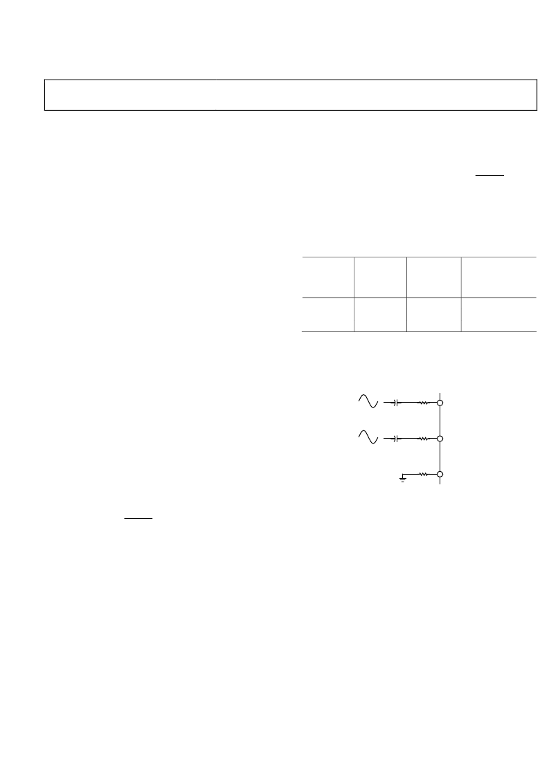
Figure 17 shows a typical configuration of the ADC inputs for
a 2.0 V
rms
input signal for a f
S
of 48 kHz. The 47 μF capacitors are
used to ac-couple the signals so that the inputs are biased at 1.5 V
ADC0/ADC1
Resistor
Value (kΩ)
7
8
18
ADC_RES
Value (kΩ)
18
18
18
NEW
S
total
f
R
_
ADC1
ADC0
ADC_RES
18k
47μF
18k
47μF
18k
ADAU1401
0
Figure 17. Audio ADC Input Configuration
相關(guān)PDF資料 |
PDF描述 |
|---|---|
| ADAU1401YSTZ-RL | SigmaDSP 28-/56-Bit Audio Processor with Two ADCs and Four DACs |
| ADAU1513 | Class-D Audio Power Stage |
| ADAU1513ACPZ | Class-D Audio Power Stage |
| ADAU1513ACPZ-RL | Class-D Audio Power Stage |
| ADAU1513ACPZ-RL7 | Class-D Audio Power Stage |
相關(guān)代理商/技術(shù)參數(shù) |
參數(shù)描述 |
|---|---|
| ADAU1401YSTZ-RL | 功能描述:IC AUDIO PROC 28/56BIT 48LQFP RoHS:是 類別:集成電路 (IC) >> 線性 - 音頻處理 系列:SigmaDSP® 其它有關(guān)文件:STA321 View All Specifications 標(biāo)準(zhǔn)包裝:1 系列:Sound Terminal™ 類型:音頻處理器 應(yīng)用:數(shù)字音頻 安裝類型:表面貼裝 封裝/外殼:64-LQFP 裸露焊盤 供應(yīng)商設(shè)備封裝:64-LQFP EP(10x10) 包裝:Digi-Reel® 其它名稱:497-11050-6 |
| ADAU1421YSTZ | 制造商:Analog Devices 功能描述: |
| ADAU1421YSTZ-REEL | 制造商:Analog Devices 功能描述: |
| ADAU1442 | 制造商:AD 制造商全稱:Analog Devices 功能描述:SigmaDSP Digital Audio Processor |
| ADAU1442YSVZ-3A | 功能描述:IC SIGMADSP 28B 175MHZ 100TQFP RoHS:是 類別:集成電路 (IC) >> 線性 - 音頻處理 系列:SigmaDSP® 其它有關(guān)文件:STA321 View All Specifications 標(biāo)準(zhǔn)包裝:1 系列:Sound Terminal™ 類型:音頻處理器 應(yīng)用:數(shù)字音頻 安裝類型:表面貼裝 封裝/外殼:64-LQFP 裸露焊盤 供應(yīng)商設(shè)備封裝:64-LQFP EP(10x10) 包裝:Digi-Reel® 其它名稱:497-11050-6 |
發(fā)布緊急采購,3分鐘左右您將得到回復(fù)。