- 您現(xiàn)在的位置:買賣IC網(wǎng) > PDF目錄384089 > ADC1010S125HN (NXP Semiconductors N.V.) Single 10-bit ADC up to 125 Msps, CMOS or LVDS DDR digital outputs PDF資料下載
參數(shù)資料
| 型號(hào): | ADC1010S125HN |
| 廠商: | NXP Semiconductors N.V. |
| 元件分類: | 外設(shè)及接口 |
| 英文描述: | Single 10-bit ADC up to 125 Msps, CMOS or LVDS DDR digital outputs |
| 封裝: | ADC1010S125HN/C1<SOT618-1 (HVQFN40)|<<http://www.nxp.com/packages/SOT618-1.html<1<Always Pb-free,;ADC1010S125HN/C1<SOT618-1 (HVQFN40)|<<http://www.nxp.com/packages/SOT618 |
| 文件頁(yè)數(shù): | 9/39頁(yè) |
| 文件大小: | 296K |
| 代理商: | ADC1010S125HN |
第1頁(yè)第2頁(yè)第3頁(yè)第4頁(yè)第5頁(yè)第6頁(yè)第7頁(yè)第8頁(yè)當(dāng)前第9頁(yè)第10頁(yè)第11頁(yè)第12頁(yè)第13頁(yè)第14頁(yè)第15頁(yè)第16頁(yè)第17頁(yè)第18頁(yè)第19頁(yè)第20頁(yè)第21頁(yè)第22頁(yè)第23頁(yè)第24頁(yè)第25頁(yè)第26頁(yè)第27頁(yè)第28頁(yè)第29頁(yè)第30頁(yè)第31頁(yè)第32頁(yè)第33頁(yè)第34頁(yè)第35頁(yè)第36頁(yè)第37頁(yè)第38頁(yè)第39頁(yè)
xxxxxxxxxxxxxxxxxxxxx xxxxxxxxxxxxxxxxxxxxxxxxxx xxxxxxx x x x xxxxxxxxxxxxxxxxxxxxxxxxxxxxxx xxxxxxxxxxxxxxxxxxx xx xx xxxxx
xxxxxxxxxxxxxxxxxxxxxxxxxxx xxxxxxxxxxxxxxxxxxx xxxxxx xxxxxxxxxxxxxxxxxxxxxxxxxxxxxxxxxxx xxxxxxxxxxxx x x
xxxxxxxxxxxxxxxxxxxxx xxxxxxxxxxxxxxxxxxxxxxxxxxxxxx xxxxx xxxxxxxxxxxxxxxxxxxxxxxxxxxxxxxxxxxxxxxxxxxxxxxxxx xxxxxxxx
xxxxxxxxxxxxxxxxxxxxxxxxx xxxxxxxxxxxxxxxxxxxx xxx
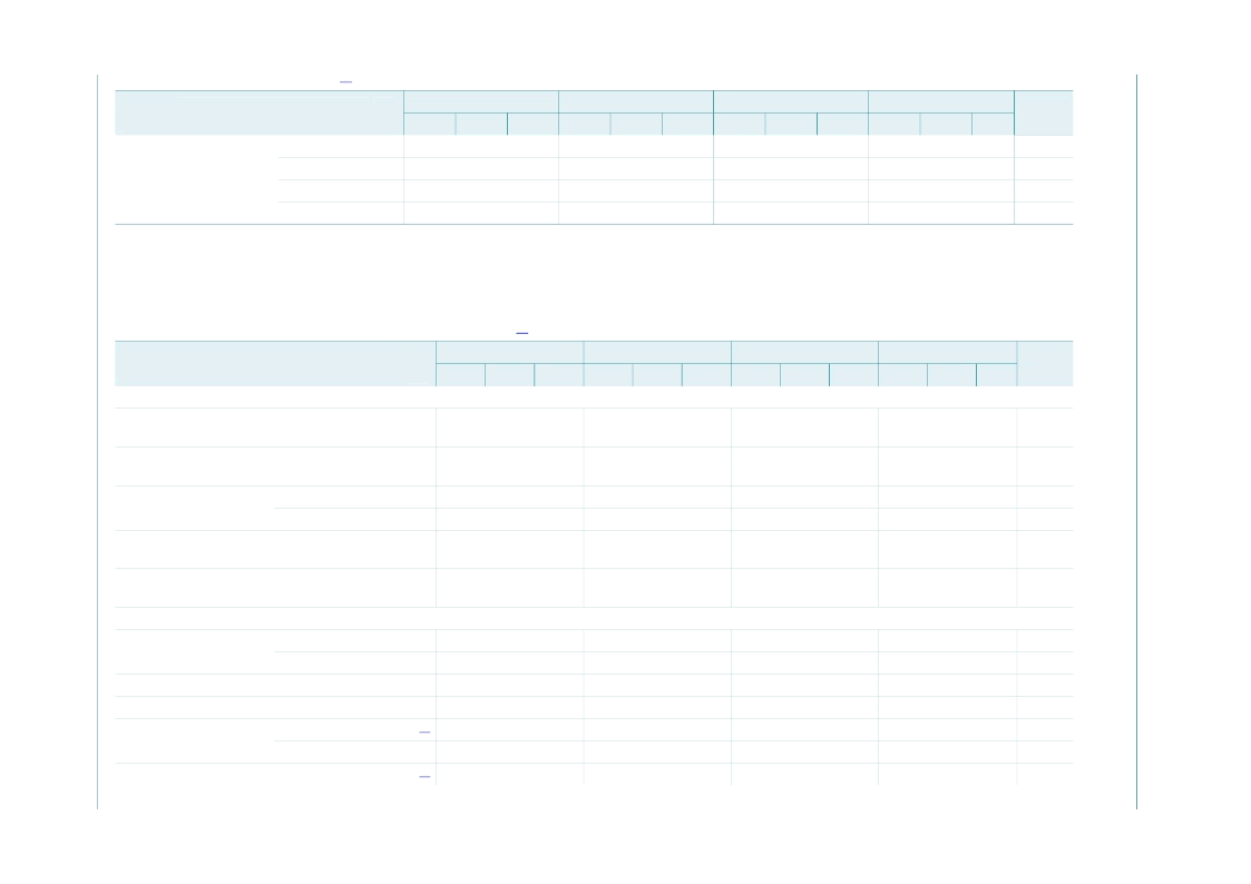
Dynamic characteristics
[1]
…continued
Parameter
Conditions
ADC1010S065
ADC1010S080
Min
Typ
Max
Min
Typ
A
A
P
R
9
N
A
S
[1]
Typical values measured at V
DDA
= 3 V, V
DDO
= 1.8 V, T
amb
= 25
°
C and C
L
= 5 pF; minimum and maximum values are across the full temperature range T
amb
=
40
°
C to +85
°
C
at V
DDA
= 3 V, V
DDO
= 1.8 V; V
INP
V
INM
=
1 dBFS; internal reference mode; applied to CMOS and LVDS interface; unless otherwise specified.
10.2 Clock and digital output timing
IMD
Intermodulation
distortion
f
i
= 3 MHz
f
i
= 30 MHz
f
i
= 70 MHz
f
i
= 170 MHz
-
-
-
-
89
88
87
84
-
-
-
-
-
-
-
-
89
88
87
85
-
-
-
-
-
-
-
-
92
92
90
87
-
-
-
-
-
-
-
-
93
92
90
88
-
-
-
-
dBc
dBc
dBc
dBc
Table 7.
Symbol
ADC1010S105
Min
Typ
ADC1010S125
Min
Unit
Max
Max
Typ
Max
Table 8.
Symbol
Clock input and digital output timing characteristics
[1]
Parameter
Conditions
ADC1010S065
Min
Typ
ADC1010S080
Min
Typ
ADC1010S105
Min
Typ
ADC1010S125
Min
Typ
Unit
Max
Max
Max
Max
Clock timing input: pins CLKP and CLKM
f
clk
clock
frequency
t
lat(data)
data latency
time
δ
clk
clock duty
cycle
40
-
65
60
-
80
75
-
105
100
-
125
MHz
-
13.5
-
-
13.5
-
-
13.5
-
-
13.5
-
clock
cycles
%
%
ns
DCS_EN = logic 1
DCS_EN = logic 0
30
45
-
50
50
0.8
70
55
-
30
45
-
50
50
0.8
70
55
-
30
45
-
50
50
0.8
70
55
-
30
45
-
50
50
0.8
70
55
-
t
d(s)
sampling
delay time
wake-up
time
t
wake
-
76
-
-
76
-
-
76
-
-
76
-
μ
s
CMOS Mode timing output: pins D9 to D0 and DAV
t
PD
propagation
delay
DAV
t
su
set-up time
t
h
hold time
t
r
rise time
DATA
DAV
t
f
fall time
DATA
DATA
13.6
-
-
-
0.39
0.26
0.19
14.9
4.2
12.5
3.4
-
-
-
16.4
-
-
-
2.4
2.4
2.4
11.9
-
-
-
0.39
0.26
0.19
12.9
3.6
9.8
3.3
-
-
-
14.4
-
-
-
2.4
2.4
2.4
8.0
-
-
-
0.39
0.26
0.19
10.8
3.3
6.8
3.1
-
-
-
12.4
-
-
-
2.4
2.4
2.4
8.2
-
-
-
0.39
0.26
0.19
9.7
3.4
5.6
2.8
-
-
-
11.3
-
-
-
2.4
2.4
2.4
ns
ns
ns
ns
ns
ns
ns
[2]
[2]
相關(guān)PDF資料 |
PDF描述 |
|---|---|
| ADC1010S065 | |
| ADC1112D125HN | Dual 11-bit ADC; CMOS or LVDS DDR digital outputs |
| ADC1112D125HN | Dual 11-bit ADC; CMOS or LVDS DDR digital outputs |
| ADC1115S125HN | Single 11-bit ADC 125 Msps with Input Buffer CMOS or LVDS DDR digital outputs |
| ADC1115S125HN | Single 11-bit ADC 125 Msps with Input Buffer CMOS or LVDS DDR digital outputs |
相關(guān)代理商/技術(shù)參數(shù) |
參數(shù)描述 |
|---|---|
| ADC1010S125HN/C1 | 制造商:PHILIPS 制造商全稱:NXP Semiconductors 功能描述:Single 10-bit ADC; 65 Msps, 80 Msps, 105 Msps or 125 Msps; CMOS or LVDS DDR digital outputs |
| ADC1010S125HN/C1,5 | 功能描述:模數(shù)轉(zhuǎn)換器 - ADC 10bit 62dB 125MSPS RoHS:否 制造商:Texas Instruments 通道數(shù)量:2 結(jié)構(gòu):Sigma-Delta 轉(zhuǎn)換速率:125 SPs to 8 KSPs 分辨率:24 bit 輸入類型:Differential 信噪比:107 dB 接口類型:SPI 工作電源電壓:1.7 V to 3.6 V, 2.7 V to 5.25 V 最大工作溫度:+ 85 C 安裝風(fēng)格:SMD/SMT 封裝 / 箱體:VQFN-32 |
| ADC1010S125HN-C1 | 制造商:Integrated Device Technology Inc 功能描述:HVQFN40 - Bulk |
| ADC1012D065HN/C1,5 | 功能描述:IC ADC 65MHZ SOT804-3 RoHS:是 類別:集成電路 (IC) >> 數(shù)據(jù)采集 - 模數(shù)轉(zhuǎn)換器 系列:- 產(chǎn)品培訓(xùn)模塊:Lead (SnPb) Finish for COTS Obsolescence Mitigation Program 標(biāo)準(zhǔn)包裝:2,500 系列:- 位數(shù):12 采樣率(每秒):3M 數(shù)據(jù)接口:- 轉(zhuǎn)換器數(shù)目:- 功率耗散(最大):- 電壓電源:- 工作溫度:- 安裝類型:表面貼裝 封裝/外殼:SOT-23-6 供應(yīng)商設(shè)備封裝:SOT-23-6 包裝:帶卷 (TR) 輸入數(shù)目和類型:- |
發(fā)布緊急采購(gòu),3分鐘左右您將得到回復(fù)。