- 您現(xiàn)在的位置:買賣IC網(wǎng) > PDF目錄378281 > ADC10158 (National Semiconductor Corporation) Low-Voltage High-Speed Quadruple Differential Line Receiver 16-SOIC 0 to 70 PDF資料下載
參數(shù)資料
| 型號(hào): | ADC10158 |
| 廠商: | National Semiconductor Corporation |
| 英文描述: | Low-Voltage High-Speed Quadruple Differential Line Receiver 16-SOIC 0 to 70 |
| 中文描述: | 10位帶符號(hào)4レs的4模數(shù)轉(zhuǎn)換器-或8通道多路復(fù)用器,采樣/保持和參考 |
| 文件頁(yè)數(shù): | 19/23頁(yè) |
| 文件大?。?/td> | 439K |
| 代理商: | ADC10158 |
第1頁(yè)第2頁(yè)第3頁(yè)第4頁(yè)第5頁(yè)第6頁(yè)第7頁(yè)第8頁(yè)第9頁(yè)第10頁(yè)第11頁(yè)第12頁(yè)第13頁(yè)第14頁(yè)第15頁(yè)第16頁(yè)第17頁(yè)第18頁(yè)當(dāng)前第19頁(yè)第20頁(yè)第21頁(yè)第22頁(yè)第23頁(yè)
2.0 Applications Information
(Continued)
The minimum value of V
(V
= V
REF+
V
REF
) can be
quite small (see Typical Performance Characteristics) to al-
low direct conversion of transducer outputs providing less
than a 5V output span. Particular care must be taken with re-
gard to noise pickup, circuit layout and system error voltage
sources when operating with a reduced span due to the in-
creased sensitivity of the converter (1 LSB equals V
REF
/2
n
).
2.3 THE ANALOG INPUTS
Due to the sampling nature of the analog inputs, at the clock
edges short duration spikes of current will be seen on the se-
lected assigned negative input. Input bypass capacitors
should not be used if the source resistance is greater than
1 k
since they will average the AC current and cause an ef-
fective DC current to flow through the analog input source re-
sistance. An op amp RC active lowpass filter can provide
both impedance buffering and noise filtering should a high
impedance signal source be required. Bypass capacitors
may be used when the source impedance is very low without
any degradation in performance.
In a true differential input stage, a signal that is common to
both “+” and “” inputs is cancelled. For the ADC10154 and
ADC10158, the positive input of a selected channel pair is
only sampled once before the start of a conversion during
the acquisition time (t
). The negative input needs to be
stable during the complete conversion sequence because it
is sampled before each decision in the SAR sequence.
Therefore, anyAC common-mode signal present on the ana-
log inputs will not be completely cancelled and will cause
some conversion errors. For a sinusoid common-mode sig-
nal this error is:
V
error
(Max) = V
PEAK
(2
π
f
CM
)(t
C
)
where f
is the frequency of the common-mode signal,
V
is its peak voltage value, and t
is theA/D’s maximum
conversion time (t
= 22/f
for 10-bit plus sign resolution).
For example, for a 60 Hz common-mode signal to generate
a
1
4
LSB error (1.24 mV) with a 4.5 μs conversion time, its
peak value would have to be approximately 731 mV.
2.4 OPTIONAL ADJUSTMENTS
2.4.1 Zero Error
The zero error of the A/D converter relates to the location of
the first riser of the transfer function (see Figure 1) and can
be measured by grounding the minus input and applying a
small magnitude positive or negative voltage to the plus in-
put. Zero error is the difference between actual DC input
voltage which is necessary to just cause an output digital
DS011225-21
a. Ratiometric Using the Internal Reference
DS011225-22
b. Absolute Using a 4.096V Span
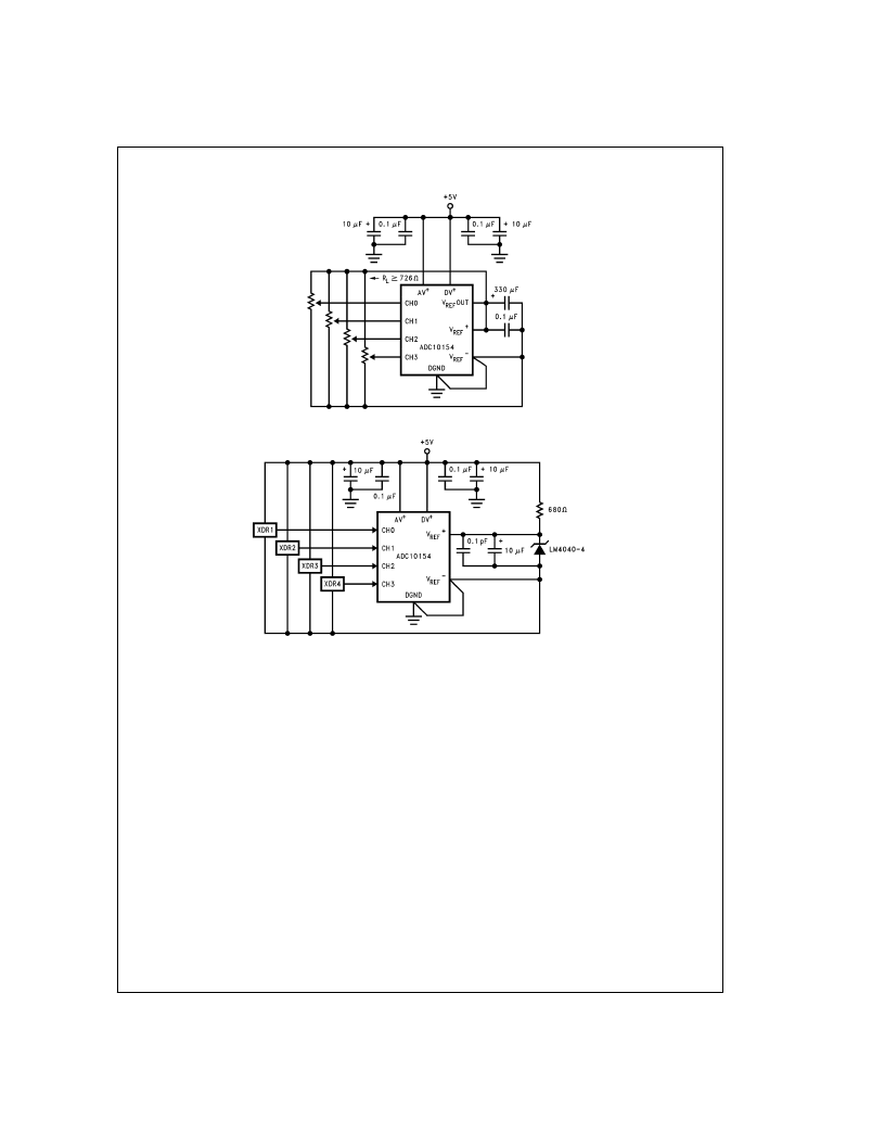
FIGURE 5. Different Reference Configurations
A
www.national.com
19
相關(guān)PDF資料 |
PDF描述 |
|---|---|
| ADC10158CIN | 10-Bit Plus Sign 4 レs ADCs with 4- or 8-Channel MUX, Track/Hold and Reference |
| ADC1021 | 10-BIT uP COMPATIBLKE A/D CONVERTERS |
| ADC1021CCJ | 10-BIT uP COMPATIBLKE A/D CONVERTERS |
| ADC1021CCJ-1 | 10-BIT uP COMPATIBLKE A/D CONVERTERS |
| ADC10221CIVT | 10-Bit, 15 MSPS, 98 mW A/D Converter with Internal Sample and Hold |
相關(guān)代理商/技術(shù)參數(shù) |
參數(shù)描述 |
|---|---|
| ADC10158BIJ | 制造商:未知廠家 制造商全稱:未知廠家 功能描述:Single-Ended Data Acquisition System |
| ADC10158CIJ | 制造商:未知廠家 制造商全稱:未知廠家 功能描述:Single-Ended Data Acquisition System |
| ADC10158CIN | 制造商:NSC 制造商全稱:National Semiconductor 功能描述:10-Bit Plus Sign 4 レs ADCs with 4- or 8-Channel MUX, Track/Hold and Reference |
| ADC10158CIN/NOPB | 功能描述:IC ADC 10BIT W/4-8 CH MX 28-DIP RoHS:是 類別:集成電路 (IC) >> 數(shù)據(jù)采集 - 模數(shù)轉(zhuǎn)換器 系列:- 產(chǎn)品培訓(xùn)模塊:Lead (SnPb) Finish for COTS Obsolescence Mitigation Program 標(biāo)準(zhǔn)包裝:2,500 系列:- 位數(shù):12 采樣率(每秒):3M 數(shù)據(jù)接口:- 轉(zhuǎn)換器數(shù)目:- 功率耗散(最大):- 電壓電源:- 工作溫度:- 安裝類型:表面貼裝 封裝/外殼:SOT-23-6 供應(yīng)商設(shè)備封裝:SOT-23-6 包裝:帶卷 (TR) 輸入數(shù)目和類型:- |
| ADC10158CIN/NOPB | 制造商:Texas Instruments 功能描述:A/D Converter (A-D) IC |
發(fā)布緊急采購(gòu),3分鐘左右您將得到回復(fù)。