- 您現(xiàn)在的位置:買賣IC網(wǎng) > PDF目錄378281 > ADC10158CIWM (NATIONAL SEMICONDUCTOR CORP) 10-Bit Plus Sign 4 レs ADCs with 4- or 8-Channel MUX, Track/Hold and Reference PDF資料下載
參數(shù)資料
| 型號: | ADC10158CIWM |
| 廠商: | NATIONAL SEMICONDUCTOR CORP |
| 元件分類: | ADC |
| 英文描述: | 10-Bit Plus Sign 4 レs ADCs with 4- or 8-Channel MUX, Track/Hold and Reference |
| 中文描述: | 8-CH 10-BIT SUCCESSIVE APPROXIMATION ADC, PARALLEL ACCESS, PDSO28 |
| 封裝: | SOP-28 |
| 文件頁數(shù): | 7/23頁 |
| 文件大小: | 439K |
| 代理商: | ADC10158CIWM |
Electrical Characteristics
(Continued)
Note 2:
Operating Ratings indicate conditions for which the device is functional, but do not guarantee specific performance limits. For guaranteed specifications and
test conditions, see the Electrical Characteristics. The guaranteed specifications apply only for the test conditions listed. Some performance characteristics may de-
grade when the device is not operated under the listed test conditions.
Note 3:
All voltages are measured with respect to GND, unless otherwise specified.
Note 4:
When the input voltage (V
) at any pin exceeds the power supplies (V
<
V
or V
>
AV
+
or DV
+
), the current at that pin should be limited to 5 mA. The
20 mA maximum package input current rating limits the number of pins that can safely exceed the power supplies with an input current of 5 mA to four.
Note 5:
The maximum power dissipation must be derated at elevated temperatures and is dictated by T
,
θ
and the ambient temperature, T
. The maximum
allowable power dissipation at any temperature is P
= (T
T
)/
θ
or the number given in the Absolute Maximum Ratings, whichever is lower. For this device,
T
= 150C. The typical thermal resistance (
θ
) of these parts when board mounted follow: ADC10154 with BIN and CIN suffixes 65C/W, ADC10154 with BIJ,
CIJ and CMJ suffixes 49C/W, ADC10154 with BIWM and CIWM suffixes 72C/W, ADC10158 with BIN and CIN suffixes 59C/W, ADC10158 with BIJ, CIJ, and CMJ
suffixes 46C/W, ADC10158 with BIWM and CIWM suffixes 68C/W.
Note 6:
Human body model, 100 pF capacitor discharged through a 1.5 k
resistor.
Note 7:
See AN-450 “Surface Mounting Methods and Their Effect on Product Reliability” or the section titled “Surface Mount” found in any post-1986 National Semi-
conductor Linear Data Book for other methods of soldering surface mount devices.
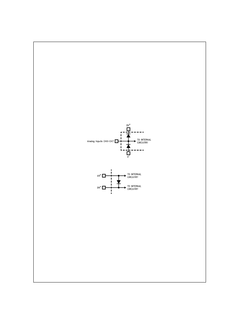
Note 8:
Two on-chip diodes are tied to each analog input as shown below. They will forward-conduct for analog input voltages one diode drop below V
supply or
one diode drop greater than V
supply. Be careful during testing at low V
levels (4.5V), as high level analog inputs (5V) can cause an input diode to conduct, es-
pecially at elevated temperatures, which will cause errors for analog inputs near full-scale. The specification allows 50 mV forward bias of either diode; this means
that as long as the analog V
does not exceed the supply voltage by more than 50 mV, the output code will be correct. Exceeding this range on an unselected chan-
nel will corrupt the reading of a selected channel. This means that if AV
and DV
are minimum (4.5 V
DC
) and V
is a maximum (4.5 V
DC
) full scale must be
≤
±
4.55
V
DC
.
Note 9:
A diode exists between AV
+
and DV
+
as shown below.
Note 10:
Typicals are at T
J
= T
A
= 25C and represent most likely parametric norm.
Note 11:
Tested limits are guaranteed to National’s AOQL (Average Outgoing Quality Level).
Note 12:
One LSB is referenced to 10 bits of resolution.
Note 13:
Total unadjusted error includes offset, full-scale, linearity, multiplexer, and hold step errors.
Note 14:
For DC Common Mode Error the only specification that is measured is offset error.
Note 15:
Channel leakage current is measured after the channel selection.
Note 16:
All the timing specifications are tested at the TTL logic levels, V
IL
= 0.8V for a falling edge and V
IH
= 2.0V for a rising.
DS011225-4
DS011225-5
To guarantee accuracy, it is required that the AV
+
and DV
+
be connected together to a power supply with separate bypass filter at each V
+
pin.
A
www.national.com
7
相關(guān)PDF資料 |
PDF描述 |
|---|---|
| ADC10154 | Low-Voltage High-Speed Quadruple Differential Line Receiver 16-SOIC 0 to 70 |
| ADC10158 | Low-Voltage High-Speed Quadruple Differential Line Receiver 16-SOIC 0 to 70 |
| ADC10158CIN | 10-Bit Plus Sign 4 レs ADCs with 4- or 8-Channel MUX, Track/Hold and Reference |
| ADC1021 | 10-BIT uP COMPATIBLKE A/D CONVERTERS |
| ADC1021CCJ | 10-BIT uP COMPATIBLKE A/D CONVERTERS |
相關(guān)代理商/技術(shù)參數(shù) |
參數(shù)描述 |
|---|---|
| ADC10158CIWM/48 | 制造商:Rochester Electronics LLC 功能描述: 制造商:Texas Instruments 功能描述: |
| ADC10158CIWM/NOPB | 功能描述:模數(shù)轉(zhuǎn)換器 - ADC RoHS:否 制造商:Texas Instruments 通道數(shù)量:2 結(jié)構(gòu):Sigma-Delta 轉(zhuǎn)換速率:125 SPs to 8 KSPs 分辨率:24 bit 輸入類型:Differential 信噪比:107 dB 接口類型:SPI 工作電源電壓:1.7 V to 3.6 V, 2.7 V to 5.25 V 最大工作溫度:+ 85 C 安裝風(fēng)格:SMD/SMT 封裝 / 箱體:VQFN-32 |
| ADC10158CIWMX | 功能描述:模數(shù)轉(zhuǎn)換器 - ADC RoHS:否 制造商:Texas Instruments 通道數(shù)量:2 結(jié)構(gòu):Sigma-Delta 轉(zhuǎn)換速率:125 SPs to 8 KSPs 分辨率:24 bit 輸入類型:Differential 信噪比:107 dB 接口類型:SPI 工作電源電壓:1.7 V to 3.6 V, 2.7 V to 5.25 V 最大工作溫度:+ 85 C 安裝風(fēng)格:SMD/SMT 封裝 / 箱體:VQFN-32 |
| ADC10158CIWMX/NOPB | 功能描述:模數(shù)轉(zhuǎn)換器 - ADC RoHS:否 制造商:Texas Instruments 通道數(shù)量:2 結(jié)構(gòu):Sigma-Delta 轉(zhuǎn)換速率:125 SPs to 8 KSPs 分辨率:24 bit 輸入類型:Differential 信噪比:107 dB 接口類型:SPI 工作電源電壓:1.7 V to 3.6 V, 2.7 V to 5.25 V 最大工作溫度:+ 85 C 安裝風(fēng)格:SMD/SMT 封裝 / 箱體:VQFN-32 |
| ADC10158CMJ | 制造商:未知廠家 制造商全稱:未知廠家 功能描述:Single-Ended Data Acquisition System |
發(fā)布緊急采購,3分鐘左右您將得到回復(fù)。