- 您現(xiàn)在的位置:買賣IC網(wǎng) > PDF目錄378281 > ADC1038CIWM (NATIONAL SEMICONDUCTOR CORP) 10-Bit Serial I/O A/D Converter with Analog Multiplexer PDF資料下載
參數(shù)資料
| 型號: | ADC1038CIWM |
| 廠商: | NATIONAL SEMICONDUCTOR CORP |
| 元件分類: | ADC |
| 英文描述: | 10-Bit Serial I/O A/D Converter with Analog Multiplexer |
| 中文描述: | 8-CH 10-BIT SUCCESSIVE APPROXIMATION ADC, SERIAL ACCESS, PDSO20 |
| 封裝: | SOP-20 |
| 文件頁數(shù): | 10/13頁 |
| 文件大?。?/td> | 551K |
| 代理商: | ADC1038CIWM |
2.0 Functional Description
(Continued)
is low continuously, since the applied clock cannot be dis-
abled, SARS must be used to synchronize the data output
on DO and initiate a new conversion. The falling edge of
SARS sends the MSB information out on DO. The next rising
edge of the clock shifts in MUX address bitA2 on DI. The fol-
lowing clock falling edge will clock the next data bit of infor-
mation out on DO.Aconversion will be started after MUX ad-
dressing information has been loaded in (3 more clocks) and
the analog sampling time (4.5 clocks) has elapsed.
3.0 Analog Considerations
3.1 THE INPUT SAMPLE AND HOLD
The sample/hold capacitor is implemented in its capacitive
ladder structure. After the channel address is received, the
ladder is switched to sample the proper analog input. This
sampling mode is maintained for 4.5 S
cycles after the
multiplexer addressing information is loaded in. The sam-
pling of the analog input starts on S
CLK
’s 4th rising edge.
An acquisition window of 4.5 S
cycles is available to al-
low the ladder capacitance to settle to the analog input volt-
age.Any change in the analog voltage before or after the ac-
quisition window will not effect the A/D conversion result.
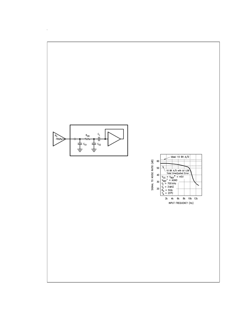
In the most simple case, the ladder’s acquisition time is de-
termined by the R
(9 k
) of the multiplexer switches, the
C
(3.5 pF) and the total ladder (C
) and stray (C
) capaci-
tance (48 pF). For large source resistance the analog input
can be modeled as an RC network as shown in Figure 1 The
values shown yield an acquisition time of about 3 μs for 10
bit accuracy with a zero to a full scale change in the reading.
External source resistance and capacitance will lengthen the
acquisition time and should be accounted for.
The curve “Signal to Noise Ratio vs Output Frequency” (Fig-
ure 2) gives an indication of the usable bandwidth. The sig-
nal to noise ratio of an idealA/D is the ratio of the RMS value
of the full scale input signal amplitude to the value of the total
error amplitude (including noise) caused by the transfer
function of the A/D. An ideal 10 bit A/D converter with a total
unadjusted error of 0 LSB would have a signal to noise ratio
of about 62 dB, which can be derived from the equation:
S/N = 6.02(N) + 1.76
where S/N is in dB and N is the number of bits. Figure 2
shows the signal to noise ratio vs. input frequency of a typi-
cal ADC1038 with
1
2
LSB total unadjusted error. The dotted
lines show signal-to-noise ratios for an ideal (noiseless) 10
bit A/D with 0 LSB error and an A/D with a 1 LSB error.
The sample-and-hold error specifications are included in the
error and timing specifications of the A/D. The hold step and
gain error sample/hold specs are taken into account in the
total unadjusted error specification, while the hold settling
time is included in the A/D’s maximum conversion time
specification. The hold droop rate can be thought of as being
zero since an unlimited amount of time can pass between a
conversion and the reading of data. However, once the data
is read it is lost and another conversion is started.
3.2 INPUT FILTERING
Due to the sampling nature of the analog input, transients
will appear on the input pins. They are caused by the ladder
capacitance and internal stray capacitance charging current
flowing into V
. These transients will not degrade the A/D’s
performance if they settle out within the sampling window.
This will occur if external source resistance is kept to a
minimum.
DS010556-18
FIGURE 1. Analog Input Model
DS010556-19
FIGURE 2. ADC1038 Signal to
Noise Ratio vs Input Frequency
www.national.com
10
相關(guān)PDF資料 |
PDF描述 |
|---|---|
| ADC1038 | 10-Bit Serial I/O A/D Converter with Analog Multiplexer |
| ADC10461 | 10-Bit 600 ns A/D Converter with Input Multiplexer and Sample/Hold |
| ADC10461CIWM | 10-Bit 600 ns A/D Converter with Input Multiplexer and Sample/Hold |
| ADC10462CIWM | 10-Bit 600 ns A/D Converter with Input Multiplexer and Sample/Hold |
| ADC10464CIWM | 10-Bit 600 ns A/D Converter with Input Multiplexer and Sample/Hold |
相關(guān)代理商/技術(shù)參數(shù) |
參數(shù)描述 |
|---|---|
| ADC104 | 制造商:MPSIND 制造商全稱:MPS Industries, Inc. 功能描述:1W, Miniature SIP, Single & Dual Output DC/DC Converters |
| ADC-10-4 | 制造商:MINI 制造商全稱:Mini-Circuits 功能描述:Directional Coupler 50Ω 5 to 1000 MHz |
| ADC-10-4+ | 制造商:MINI 制造商全稱:Mini-Circuits 功能描述:Directional Coupler 50Ω 5 to 1000 MHz |
| ADC10461 | 制造商:NSC 制造商全稱:National Semiconductor 功能描述:10-Bit 600 ns A/D Converter with Input Multiplexer and Sample/Hold |
| ADC10461_06 | 制造商:NSC 制造商全稱:National Semiconductor 功能描述:10-Bit 600 ns A/D Converter with Input Multiplexer and Sample/Hold |
發(fā)布緊急采購,3分鐘左右您將得到回復(fù)。