- 您現(xiàn)在的位置:買賣IC網(wǎng) > PDF目錄378282 > ADC10662CIWM (NATIONAL SEMICONDUCTOR CORP) RES 12-OHM 5% 0.25W 200PPM THK-FILM SMD-1206 TR-7-PA PDF資料下載
參數(shù)資料
| 型號: | ADC10662CIWM |
| 廠商: | NATIONAL SEMICONDUCTOR CORP |
| 元件分類: | ADC |
| 英文描述: | RES 12-OHM 5% 0.25W 200PPM THK-FILM SMD-1206 TR-7-PA |
| 中文描述: | 2-CH 10-BIT FLASH/SUCCESSIVE APPROXIMATION ADC, PARALLEL ACCESS, PDSO24 |
| 封裝: | SO-24 |
| 文件頁數(shù): | 5/14頁 |
| 文件大小: | 274K |
| 代理商: | ADC10662CIWM |
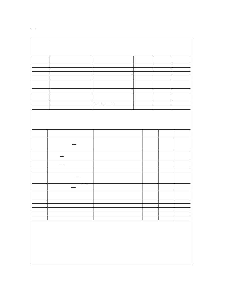
DC Electrical Characteristics
The following specifications apply for V
+
= +5V, V
REF(+)
= 5V V
REF()
= GND, and Speed Adjust pin connected to ground
through a 14.0 k
resistor (Mode 1) or an 8.26 k
Boldface limits apply for
T
A
= T
J
= T
MIN
to T
MAX
;
all other limits T
A
= T
J
= +25C.
Symbol
Parameter
Conditions
Typical
(Note 7)
Limit
(Note 8)
2.0
0.8
3.0
3.0
2.4
4.25
0.4
50
50
2
45
Units
(Limits)
V (min)
V (max)
μA (max)
μA (max)
V (min)
V (min)
V (max)
μA (max)
μA (max)
mA (max)
mA (max)
V
IN(1)
V
IN(0)
I
IN(1)
I
IN(0)
V
OUT(1)
Logical “1” Input Voltage
Logical “0” Input Voltage
Logical “1” Input Current
Logical “0” Input Current
Logical “1” Output Voltage
V
+
= 5.5V
V
+
= 4.5V
V
IN(1)
= 5V
V
IN(0)
0V
V
+
= 4.5V, I
OUT
= 360 μA
V
+
= 4.5V, I
OUT
= 10 μA
V
+
= 4.5V, I
OUT
= 1.6 mA
V
OUT
= 5V
V
OUT
= 0V
CS = S /H = RD = 0
CS = S /H = RD = 0
0.005
0.005
V
OUT(0)
I
OUT
Logical “0” Output Voltage
TRI-STATE
Output Current
0.1
0.1
1.0
30
DI
CC
AI
CC
DV
CC
Supply Current
AV
CC
Supply Current
AC Electrical Characteristics
The following specifications apply for V
+
= +5V, t
= t
= 20 ns, V
REF(+)
= 5V, V
= GND, and Speed Adjust pin con-
nected to ground through a 14.0 k
resistor (Mode 1) or an 8.26 k
resistor (Mode 2) unless otherwise specified.
Boldface
limits apply for T
A
= T
J
= T
MIN
to T
MAX
;
all other limits T
A
= T
J
= +25C.
Symbol
Parameter
Conditions
Typical
(Note 7)
Limit
(Note 8)
Units
(Limits)
t
CONV
Mode 1 Conversion Time
from Rising Edge of S /H
to Falling Edge of INT
Mode 2 Conversion Time
Access Time (Delay from Falling
Edge of RD to Output Valid)
Access Time (Delay from Falling
Edge of RD to Output Valid)
Minimum Sample Time
TRI-STATE Control (Delay
from Rising Edge of RD
to High-Z State)
Delay from Rising Edge of RD
to Rising Edge of INT
Delay from End of Conversion
to Next Conversion
Multiplexer Control Setup Time
Multiplexer Hold Time
Analog Input Capacitance
Logic Output Capacitance
Logic Input Capacitance
360
466
ns (max)
t
CRD
470
610
ns (max)
t
ACC1
Mode 1; C
L
= 100 pF
30
50
ns (max)
t
ACC2
Mode 2; C
L
= 100 pF
475
616
ns (max)
t
SH
Mode 1 (Figure 1 ) ; (Note 9)
R
L
= 1k, C
L
= 10 pF
150
ns (max)
t
1H
, t
0H
30
60
ns (max)
t
INTH
C
L
= 100 pF
25
50
ns (max)
t
P
50
ns (max)
t
MS
t
MH
C
VIN
C
OUT
C
IN
10
10
35
5
5
75
40
ns (max)
ns (max)
pF (max)
pF (max)
pF (max)
Note 1:
Absolute Maximum Ratings indicate limits beyond which damage to the device may occur. Operating Ratings indicate conditions for which the device is func-
tional. These ratings do not guarantee specific performance limits, however. For guaranteed specifications and test conditions, see the Electrical Characteristics. The
guaranteed specifications apply only for the test conditions listed. Some performance characteristics may degrade when the device is not operated under the listed
test conditons.
Note 2:
All voltages are measured with respect to GND, unless otherwise specified.
Note 3:
When the input voltage (V
IN
) at any pin exceeds the power supply rails (V
IN
<
GND or V
IN
>
V
+
) the absolute value of current at that pin should be limited
to 5 mA or less. The 20 mA package input current limits the number of pins that can safely exceed the power supplies with an input current of 5 mA to four.
Note 4:
The maximum power dissipation must be derated at elevated temperatures and is dictated by T
,
θ
and the ambient temperature, T
. The maximum
allowable power dissipation at any temperature is P
= (T
T
)/
θ
or the number given in the Absolute Maximum Ratings, whichever is lower. In most cases,
the maximum derated power dissipation will be reached only during fault conditions. For these devices, T
JMAX
for a board-mounted device can be found from the
tables below:
www.national.com
5
相關(guān)PDF資料 |
PDF描述 |
|---|---|
| ADC10662 | 10-Bit 360 ns A/D Converter with Input Multiplexer and Sample/Hold |
| ADC10664 | Switch-mode Multi-Chemistry Battery Charger with Peak Voltage Detection Termination 8-SOIC -20 to 70 |
| ADC10664CIWM | 10-Bit 360 ns A/D Converter with Input Multiplexer and Sample/Hold |
| ADC10734 | 10-Bit Plus Sign Serial I/O A/D Converters with Mux,Sample/Hold and Reference(10位串行輸入/輸出帶MUX,采樣/保持和參考功能的A/D轉(zhuǎn)換器) |
| ADC10732 | 10-Bit Plus Sign Serial I/O A/D Converters with Mux, |
相關(guān)代理商/技術(shù)參數(shù) |
參數(shù)描述 |
|---|---|
| ADC10662CIWM/NOPB | 功能描述:IC ADC 10BIT 360 NS 24-SOIC RoHS:是 類別:集成電路 (IC) >> 數(shù)據(jù)采集 - 模數(shù)轉(zhuǎn)換器 系列:- 產(chǎn)品培訓(xùn)模塊:Lead (SnPb) Finish for COTS Obsolescence Mitigation Program 標(biāo)準(zhǔn)包裝:2,500 系列:- 位數(shù):12 采樣率(每秒):3M 數(shù)據(jù)接口:- 轉(zhuǎn)換器數(shù)目:- 功率耗散(最大):- 電壓電源:- 工作溫度:- 安裝類型:表面貼裝 封裝/外殼:SOT-23-6 供應(yīng)商設(shè)備封裝:SOT-23-6 包裝:帶卷 (TR) 輸入數(shù)目和類型:- |
| ADC10662CIWMX | 功能描述:IC ADC 10BIT 24-SOIC RoHS:是 類別:集成電路 (IC) >> 數(shù)據(jù)采集 - 模數(shù)轉(zhuǎn)換器 系列:- 產(chǎn)品培訓(xùn)模塊:Lead (SnPb) Finish for COTS Obsolescence Mitigation Program 標(biāo)準(zhǔn)包裝:2,500 系列:- 位數(shù):12 采樣率(每秒):3M 數(shù)據(jù)接口:- 轉(zhuǎn)換器數(shù)目:- 功率耗散(最大):- 電壓電源:- 工作溫度:- 安裝類型:表面貼裝 封裝/外殼:SOT-23-6 供應(yīng)商設(shè)備封裝:SOT-23-6 包裝:帶卷 (TR) 輸入數(shù)目和類型:- |
| ADC10662CIWMX/NOPB | 制造商:Texas Instruments 功能描述:ADC Single Pipelined 1.5Msps 10-bit Parallel 24-Pin SOIC W T/R |
| ADC10662CMJ | 制造商:未知廠家 制造商全稱:未知廠家 功能描述:Single-Ended Data Acquisition System |
| ADC10664 | 制造商:NSC 制造商全稱:National Semiconductor 功能描述:10-Bit 360 ns A/D Converter with Input Multiplexer and Sample/Hold |
發(fā)布緊急采購,3分鐘左右您將得到回復(fù)。