- 您現(xiàn)在的位置:買賣IC網(wǎng) > PDF目錄378283 > ADC12041 (National Semiconductor Corporation) 12-Bit Plus Sign 216 kHz Sampling Analog-to-Digital Converter(12位216 kHz采樣A/D轉(zhuǎn)換器) PDF資料下載
參數(shù)資料
| 型號: | ADC12041 |
| 廠商: | National Semiconductor Corporation |
| 英文描述: | 12-Bit Plus Sign 216 kHz Sampling Analog-to-Digital Converter(12位216 kHz采樣A/D轉(zhuǎn)換器) |
| 中文描述: | 12位帶符號216 kHz的采樣模擬到數(shù)字轉(zhuǎn)換器(12位216 kHz的采樣的A / D轉(zhuǎn)換器) |
| 文件頁數(shù): | 7/28頁 |
| 文件大小: | 591K |
| 代理商: | ADC12041 |
第1頁第2頁第3頁第4頁第5頁第6頁當前第7頁第8頁第9頁第10頁第11頁第12頁第13頁第14頁第15頁第16頁第17頁第18頁第19頁第20頁第21頁第22頁第23頁第24頁第25頁第26頁第27頁第28頁
Digital Timing Characteristics
(Continued)
The following specifications apply to the ADC12041, 13-bit data bus width, V
A
+ = V
D
+ = 5V, f
CLK
= 12 MHz, t
f
= 3 ns and C
L
= 50 pF on data I/O lines
Symbol
Parameter
Conditions
Typical
(Note 10)
Limits
(Note 11)
Unit
(Limit)
t
RDRDY
Rising Edge of RD
to Rising Edge of RDY
Active Edge of WR
to Rising Edge of RDY
Active Edge of WR
to Falling Edge of RDY
24
38
ns (max)
t
WRRDY
WMODE = “1”
37
60
ns (max)
t
STDRDY
WMODE = “0”. Writing the
RESET Command into the
Configuration Register
1.4
2.5
ms (max)
t
SYNC
Minimum SYNC Pulse Width
5
10
ns (min)
Notes on Specifications
Note 1:
Absolute Maximum Ratings indicate limits beyond which damage to the device may occur. Operating Ratings indicate conditions for which the device is
functional, but do not guarantee specific performance limits. For guaranteed specifications and test conditions, see the Electrical Characteristics. The guaranteed
specifications apply only for the test conditions listed. Some performance characteristics may degrade when the device is not operated under the listed test condi-
tions.
Note 2:
All voltages are measured with respect to GND, unless otherwise specified.
Note 3:
When the input voltage (V
) at any pin exceeds the power supply rails (V
<
GND or V
>
(V
+ or V
+)), the current at that pin should be limited to 30
mA. The 120 mA maximum package input current limits the number of pins that can safely exceed the power supplies with an input current of 30 mA to four.
Note 4:
The maximum power dissipation must he derated at elevated temperatures and is dictated by T
, (maximum junction temperature),
θ
JA
(package junc-
tion to ambient thermal resistance), and T
(ambient temperature). The maximum allowable power dissipation at any temperature is P
= (T
T
)/
θ
or
the number given in the Absolute Maximum Ratings, whichever is lower. For this device, T
= 150C, and the typical thermal resistance (
θ
JA
) of the ADC12041
in the V package, when board mounted, is 55C/W, and in the SSOP package, when board mounted, is 130C/W.
Note 5:
Human body model, 100 pF discharged through 1.5
k resistor.
Note 6:
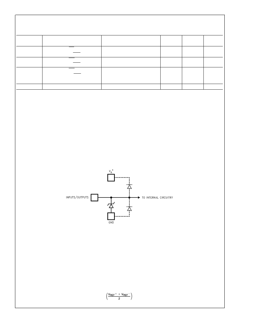
Each input is protected by a nominal 6.5V breakdown voltage zener diode to GND, as shown below, input voltage magnitude up to 5V above V
+ or 5V
below GND will not damage the ADC12041. There are parasitic diodes that exist between the inputs and the power supply rails and errors in the A/D conversion
can occur if these diodes are forward biased by more than 50 mV. As an example, if V
A
+ is 4.50 V
DC
, full-scale input voltage must be 4.55 V
DC
to ensure accurate
conversions.
Note 7:
V
+ and V
+ must be connected together to the same power supply voltage and bypassed with separate capacitors at each V
+
pin to assure conversion/
comparison accuracy. Refer to the Power Supply Considerations section for a detailed discussion.
Note 8:
Accuracy is guaranteed when operating at f
CLK
= 12 MHz.
Note 9:
With the test condition for V
REF
(V
REF
+ V
REF
) given as + 4.096V, the 12-bit LSB is 1.000 mV.
Note 10:
Typicals are at T
A
= 25C and represent most likely parametric norm.
Note 11:
Limits are guaranteed to National’s AOQL (Average Outgoing Quality Level).
Note 12:
Positive integral linearity error is defined as the deviation of the analog value, expressed in LSBs, from the straight line that passes through positive
full-scale and zero. For negative integral linearity error, the straight line passes through negative full-scale and zero.
Note 13:
Zero error is a measure of the deviation from the mid-scale voltage (a code of zero), expressed in LSB. It is the average value of the code transitions be-
tween 1 to 0 and 0 to + 1 (see Figure 8).
Note 14:
The DC common-mode error is measured with both inputs shorted together and driven from 0V to 5V. The measured value is referred to the resulting out-
put value when the inputs are driven with a 2.5V input.
Note 15:
Power Supply Sensitivity is measured after an Auto-Zero and Auto Calibration cycle has been completed with V
A
+ and V
D
+ at the specified extremes.
Note 16:
V
REFCM
(Reference Voltage Common Mode Range) is defined as
DS012441-4
A
www.national.com
7
相關(guān)PDF資料 |
PDF描述 |
|---|---|
| ADC12041CIV | 12-Bit Plus Sign 216 kHz Sampling Analog-to-Digital Converter |
| ADC12041CIMSA | NiCd/NiMH/Lead-Acid Gas Gauge For High Discharge Rates (>10A), Pgmable Offset Error & Load Comp. 16-SOIC 0 to 70 |
| ADC12048EVAL | 12-Bit Plus Sign 216 kHz 8-Channel Sampling Analog-to-Digital Converter |
| ADC12048CIVF | 12-Bit Plus Sign 216 kHz 8-Channel Sampling Analog-to-Digital Converter |
| ADC12048 | 12-Bit Plus Sign 216 kHz 8-Channel Sampling Analog-to-Digital Converter |
相關(guān)代理商/技術(shù)參數(shù) |
參數(shù)描述 |
|---|---|
| ADC12041AZ WAF | 制造商:Texas Instruments 功能描述: |
| ADC12041CIMSA | 制造商:NSC 制造商全稱:National Semiconductor 功能描述:12-Bit Plus Sign 216 kHz Sampling Analog-to-Digital Converter |
| ADC12041CIMSAX | 功能描述:IC ADC 12BIT 28-SSOP RoHS:否 類別:集成電路 (IC) >> 數(shù)據(jù)采集 - 模數(shù)轉(zhuǎn)換器 系列:- 產(chǎn)品培訓模塊:Lead (SnPb) Finish for COTS Obsolescence Mitigation Program 標準包裝:2,500 系列:- 位數(shù):12 采樣率(每秒):3M 數(shù)據(jù)接口:- 轉(zhuǎn)換器數(shù)目:- 功率耗散(最大):- 電壓電源:- 工作溫度:- 安裝類型:表面貼裝 封裝/外殼:SOT-23-6 供應商設備封裝:SOT-23-6 包裝:帶卷 (TR) 輸入數(shù)目和類型:- |
| ADC12041CIV | 制造商:NSC 制造商全稱:National Semiconductor 功能描述:12-Bit Plus Sign 216 kHz Sampling Analog-to-Digital Converter |
| ADC12041CIVX | 制造商:NSC 制造商全稱:National Semiconductor 功能描述:12-Bit Plus Sign 216 kHz Sampling Analog-to-Digital Converter |
發(fā)布緊急采購,3分鐘左右您將得到回復。