- 您現(xiàn)在的位置:買賣IC網 > PDF目錄376484 > AM29BL802C90RZK (Spansion Inc.) 8 Megabit (512 K x 16-Bit) CMOS 3.0 Volt-only Burst Mode Flash Memory PDF資料下載
參數(shù)資料
| 型號: | AM29BL802C90RZK |
| 廠商: | Spansion Inc. |
| 英文描述: | 8 Megabit (512 K x 16-Bit) CMOS 3.0 Volt-only Burst Mode Flash Memory |
| 中文描述: | 8兆位(512畝× 16位)的CMOS 3.0伏特,只有突發(fā)模式閃存 |
| 文件頁數(shù): | 16/46頁 |
| 文件大?。?/td> | 466K |
| 代理商: | AM29BL802C90RZK |
第1頁第2頁第3頁第4頁第5頁第6頁第7頁第8頁第9頁第10頁第11頁第12頁第13頁第14頁第15頁當前第16頁第17頁第18頁第19頁第20頁第21頁第22頁第23頁第24頁第25頁第26頁第27頁第28頁第29頁第30頁第31頁第32頁第33頁第34頁第35頁第36頁第37頁第38頁第39頁第40頁第41頁第42頁第43頁第44頁第45頁第46頁

14
Am29BL802C
22371C7 November 3, 2006
D A T A S H E E T
Temporary Sector Unprotect
This feature allows temporary unprotection of previ-
ously protected sectors to change data in-system. The
Sector Unprotect mode is activated by setting the RE-
SET# pin to V
ID
. During this mode, formerly protected
sectors can be programmed or erased by selecting the
sector addresses. Once V
ID
is removed from the RE-
SET# pin, all the previously protected sectors are
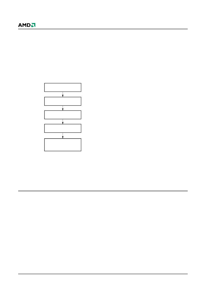
protected again. Figure 2 shows the algorithm, and
Figure 23 shows the timing diagrams, for this feature.
HARDWARE DATA PROTECTION
The command sequence requirement of unlock cycles
for programming or erasing provides data protection
against inadvertent writes (refer to Table 4 for com-
mand definitions). In addition, the following hardware
data protection measures prevent accidental erasure
or programming, which might otherwise be caused by
spurious system level signals during V
CC
power-up and
power-down transitions, or from system noise.
Low V
CC
Write Inhibit
When V
CC
is less than V
LKO
, the device does not ac-
cept any write cycles. This protects data during V
CC
power-up and power-down. The command register and
all internal program/erase circuits are disabled, and the
device resets. Subsequent writes are ignored until V
CC
is greater than V
LKO
. The system must provide the
proper signals to the control pins to prevent uninten-
tional writes when V
CC
is greater than V
LKO
.
Write Pulse “Glitch” Protection
Noise pulses of less than 5 ns (typical) on OE#, CE# or
WE# do not initiate a write cycle.
Logical Inhibit
Write cycles are inhibited by holding any one of OE# =
V
IL
, CE# = V
IH
or WE# = V
IH
. To initiate a write cycle,
CE# and WE# must be a logical zero while OE# is a
logical one.
Power-Up Write Inhibit
If WE# = CE# = V
IL
and OE# = V
IH
during power up, the
device does not accept commands on the rising edge
of WE#. The internal state machine is automatically
reset to reading array data on power-up.
COMMAND DEFINITIONS
Writing specific address and data commands or se-
quences into the command register initiates device op-
erations. Table 4 defines the valid register command
sequences. Writing
incorrect
address and data val-
ues
or writing them in the
improper sequence
resets
the device to reading array data.
All addresses are latched on the falling edge of
WE# or CE#, whichever happens later. All data is
latched on the rising edge of WE# or CE#, whichever
happens first. Refer to the appropriate timing diagrams
in the AC Characteristics section.
Reading Array Data in Non-burst Mode
The device is automatically set to reading array data
after device power-up. No commands are required to
retrieve data. The device is also ready to read array
data after completing an Embedded Program or Em-
bedded Erase algorithm.
After the device accepts an Erase Suspend com-
mand, the device enters the Erase Suspend mode.
The system can read array data using the standard
read timings, except that if it reads at an address
within erase-suspended sectors, the device outputs
status data. After completing a programming opera-
tion in the Erase Suspend mode, the system may
once again read array data with the same exception.
See “Erase Suspend/Erase Resume Commands” for
more information on this mode.
The system
must
issue the reset command to re-en-
able the device for reading array data if DQ5 goes high,
START
Perform Erase or
Program Operations
RESET# = V
IH
Temporary Sector
Unprotect Completed
(Note 2)
RESET# = V
ID
(Note 1)
Notes:
1. All protected sectors unprotected.
2. All previously protected sectors are protected once
again.
Figure 2.
Temporary Sector Unprotect Operation
相關PDF資料 |
PDF描述 |
|---|---|
| AM29BL802CB-120R | 8 Megabit (512 K x 16-Bit) CMOS 3.0 Volt-only Burst Mode Flash Memory |
| AM29BL802CB-65R | 8 Megabit (512 K x 16-Bit) CMOS 3.0 Volt-only Burst Mode Flash Memory |
| AM29BL802CB-70R | 8 Megabit (512 K x 16-Bit) CMOS 3.0 Volt-only Burst Mode Flash Memory |
| AM29BL802CB-90R | 8 Megabit (512 K x 16-Bit) CMOS 3.0 Volt-only Burst Mode Flash Memory |
| AM29LV652DU12RMAI | 128 Megabit (16 M x 8-Bit) CMOS 3.0 Volt-only Uniform Sector Flash Memory with VersatileIO Control |
相關代理商/技術參數(shù) |
參數(shù)描述 |
|---|---|
| AM29BL802CB-65RZET | 制造商:Spansion 功能描述: |
| AM29C01WW WAF | 制造商:Advanced Micro Devices 功能描述: |
| AM29C10API | 制造商:Rochester Electronics LLC 功能描述:- Bulk |
| AM29C10AWW DIE | 制造商:Advanced Micro Devices 功能描述: |
| AM29C116-1JC | 制造商:Rochester Electronics LLC 功能描述:- Bulk |
發(fā)布緊急采購,3分鐘左右您將得到回復。