- 您現(xiàn)在的位置:買賣IC網 > PDF目錄166216 > AM29LV010B-55ED (SPANSION LLC) Flash Memory IC; Leaded Process Compatible:Yes; Memory Size:10Mbit; Package/Case:32-TSOP; Peak Reflow Compatible (260 C):Yes; Supply Voltage Max:3V; Access Time, Tacc:55ns; Series:AM29 RoHS Compliant: Yes PDF資料下載
參數(shù)資料
| 型號: | AM29LV010B-55ED |
| 廠商: | SPANSION LLC |
| 元件分類: | PROM |
| 英文描述: | Flash Memory IC; Leaded Process Compatible:Yes; Memory Size:10Mbit; Package/Case:32-TSOP; Peak Reflow Compatible (260 C):Yes; Supply Voltage Max:3V; Access Time, Tacc:55ns; Series:AM29 RoHS Compliant: Yes |
| 中文描述: | 128K X 8 FLASH 3V PROM, 55 ns, PDSO32 |
| 封裝: | LEAD FREE, MO-142BD, TSOP-32 |
| 文件頁數(shù): | 6/37頁 |
| 文件大小: | 967K |
| 代理商: | AM29LV010B-55ED |
第1頁第2頁第3頁第4頁第5頁當前第6頁第7頁第8頁第9頁第10頁第11頁第12頁第13頁第14頁第15頁第16頁第17頁第18頁第19頁第20頁第21頁第22頁第23頁第24頁第25頁第26頁第27頁第28頁第29頁第30頁第31頁第32頁第33頁第34頁第35頁第36頁第37頁
14
Am29LV010B
22140D7 February 24, 2009
D A TA SH EET
generated program pulses and verify the programmed
cell margin. Table 4 shows the address and data
requirement s fo r the by te progra m command
sequence.
When the Embedded Program algorithm is complete,
the device then returns to reading array data and
addresses are no longer latched. The system can
determine the status of the program operation by using
DQ7 or DQ6. See “Write Operation Status” for informa-
tion on these status bits.
Any commands written to the device during the
Embedded Program Algorithm are ignored. The Byte
Program command sequence should be reinitiated
once the device has reset to reading array data, to
ensure data integrity.
Programming is allowed in any sequence and across
sector boundaries. A bit cannot be programmed
from a “0” back to a “1”. Attempting to do so may halt
the operation and set DQ5 to “1,” or cause the Data#
Polling algorithm to indicate the operation was suc-
cessful. However, a succeeding read will show that the
data is still “0”. Only erase operations can convert a “0”
to a “1”.
Unlock Bypass Command Sequence
The unlock bypass feature allows the system to
program bytes to the device faster than using the stan-
dard program command sequence. The unlock bypass
command sequence is initiated by first writing two
unlock cycles. This is followed by a third write cycle
containing the unlock bypass command, 20h. The
device then enters the unlock bypass mode. A two-
cycle unlock bypass program command sequence is all
that is required to program in this mode. The first cycle
in this sequence contains the unlock bypass program
command, A0h; the second cycle contains the program
address and data. Additional data is programmed in
the same manner. This mode dispenses with the initial
two unlock cycles required in the standard program
command sequence, resulting in faster total program-
ming time. Table 4 shows the requirements for the
command sequence.
During the unlock bypass mode, only the Unlock
Bypass Program and Unlock Bypass Reset commands
are valid. To exit the unlock bypass mode, the system
must issue the two-cycle unlock bypass reset
command sequence. The first cycle must contain the
data 90h; the second cycle the data 00h. Addresses
are don’t cares for both cycles. The device then returns
to reading array data.
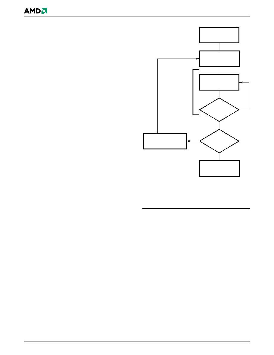
Figure 1 illustrates the algorithm for the program oper-
ation. See the Erase/Program Operations table in “AC
Characteristics” for parameters, and to Figure 12 for
timing diagrams.
Note:See Table 4 for program command sequence.
Figure 1.
Program Operation
Chip Erase Command Sequence
Chip erase is a six bus cycle operation. The chip erase
command sequence is initiated by writing two unlock
cycles, followed by a set-up command. Two additional
unlock write cycles are then followed by the chip erase
command, which in turn invokes the Embedded Erase
algorithm. The device does not require the system to
preprogram prior to erase. The Embedded Erase algo-
rithm automatically preprograms and verifies the entire
memory for an all zero data pattern prior to electrical
erase. The system is not required to provide any con-
trols or timings during these operations. Table 4 shows
the address and data requirements for the chip erase
command sequence.
Any comm ands wr it ten to th e chip dur ing th e
Embedded Erase algorithm are ignored. The Chip
Erase command sequence should be reinitiated once
the device has returned to reading array data, to
ensure data integrity.
START
Write Program
Command Sequence
Data Poll
from System
Verify Data?
No
Yes
Last Address?
No
Yes
Programming
Completed
Increment Address
Embedded
Program
algorithm
in progress
相關PDF資料 |
PDF描述 |
|---|---|
| AM29LV160DT-70FK | 1M X 16 FLASH 3V PROM, 70 ns, PDSO48 |
| AM29LV200BT-55RFC | 128K X 16 FLASH 3V PROM, 55 ns, PDSO48 |
| AM29LV256MH128EI | 16M X 16 FLASH 3V PROM, 120 ns, PDSO56 |
| AM29LV256MH118REI | 16M X 16 FLASH 3V PROM, 110 ns, PDSO56 |
| AM29PDL127H83PCIN | 128 Megabit (8 M x 16-Bit) CMOS 3.0 Volt-only, Page Mode Simultaneous Read/Write Flash Memory with Enhanced VersatileIO Control |
相關代理商/技術參數(shù) |
參數(shù)描述 |
|---|---|
| AM29LV010B-55JCT | 制造商:Spansion 功能描述:1M (128KX8) 3V, UNIFORM SECTOR, PLCC32, COM, T&R - Tape and Reel |
| AM29LV010B-70ED | 制造商:Spansion 功能描述:IC SM FLASH 3V 1MB |
| AM29LV010B-70ED | 制造商:Spansion 功能描述:FLASH MEMORY IC |
| AM29LV010B-70EI | 制造商:Advanced Micro Devices 功能描述: |
| AM29LV010B-70JC | 制造商:ADV-MICRO-DEV 功能描述: |
發(fā)布緊急采購,3分鐘左右您將得到回復。