- 您現(xiàn)在的位置:買賣IC網(wǎng) > PDF目錄379667 > AMC8500QS16 (Electronic Theatre Controls, Inc.) TWO PHASE VARIABLE SPEED FAN MOTOR CONTROLLER PDF資料下載
參數(shù)資料
| 型號(hào): | AMC8500QS16 |
| 廠商: | Electronic Theatre Controls, Inc. |
| 英文描述: | TWO PHASE VARIABLE SPEED FAN MOTOR CONTROLLER |
| 中文描述: | 兩相流變速風(fēng)扇電機(jī)控制器 |
| 文件頁數(shù): | 22/27頁 |
| 文件大?。?/td> | 648K |
| 代理商: | AMC8500QS16 |
第1頁第2頁第3頁第4頁第5頁第6頁第7頁第8頁第9頁第10頁第11頁第12頁第13頁第14頁第15頁第16頁第17頁第18頁第19頁第20頁第21頁當(dāng)前第22頁第23頁第24頁第25頁第26頁第27頁
P
P
Preliminary Specification
Andigilog, Inc. 2006
www.andigilog.com
August 2006 - 70A04018
aMC8500
- 22 -
4800
40
Control Signal Duty Cycle (%)
36
10%
20%
34
32
30
28
26
24
60
80
100
20
0
4000
3200
2400
1600
0
800
Min Speed Set
Intercept Points
Inlet Air Temperature °C
Figure 39- Fan Speed versus Control Signal Duty Cycle
for Various Inlet Air Temperatures
F
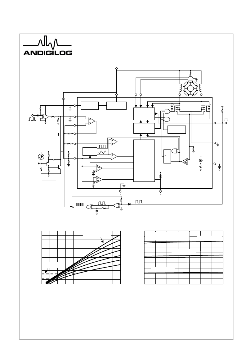
The above circuit controls fan speed in a closed loop manner that is proportional to the control signal duty cycle and inlet air
temperature. A voltage indicating the required fan speed or Reference is applied to Pin 7 and is derived from the Duty Cycle to Voltage
Converter and Temperature Controlled Clamp circuits. The Duty Cycle to Voltage Converter consists of an XOR gate buffer that drives a
10 k, 22
μ
F low pass filter, with the high state level limited by the Temperature Controlled Clamp. A voltage indicating the actual fan
speed or Feedback is applied to Pin 8 and is derived from the Frequency to Voltage Converter that consists of two XOR gates. The first
XOR buffers the FGRL tachometer signal and connects to the second which is configured as an edge transition one-shot that drives a
100 k, 330 nF low pass filter. The Op Amp compares the difference between the Reference and Feedback voltages and generates an
Error signal that drives Pin 6 in a corrective fashion causing the fan to run either faster or slower so that the Feedback voltage level
becomes the same as the Reference. Performance data is shown in the above graphs. Note that the Error signal is applied to Pin 6
instead of Pin 10 and that Pin 10 must be biased between 1.0 V to 3.0 V for proper operation.
Figure 40- Fan Speed versus Motor Voltage
for Various Control Signal Duty Cycles
600
1000
1400
1800
2200
2600
10.8
11.2
11.6
12.0
12.4
12.8
13.2
13.6
70% Duty Cycle
50% Duty Cycle
30% Duty Cycle
Control Signal = 0 to 5.0 V, 10 kHz
Inlet Air Temperature = 30°C
Motor Voltage (V)
F
FGRL
Out
Temperature
Controlled
Clamp
Thermistor
(°C)
24
25
26
28
30
32
34
36
β
= 3300
(
)
10464
10061
9712
9027
8394
7828
7291
6799
Frequency to Voltage Converter
Duty Cycle
to Voltage
Converter
Control
Signal
Input
2.8 k
150 k
10 nF
6.8 k
10 k
100 k
47 k
20 k
330 nF
1 M
15
9
Under Voltage
Lockout
Reference
Op Amp
Hall Amplifier
Non-Overlap
Commutation
Fault Timer
Power Down
Kick Start
Current
Limit
Latch
Thermal
Shutdown
R
S
Q
Current Limit
Comp
10
μ
A
PWM
Logic
Motor
Drives
Digital
Detector
Oscillator
PWM Comp
Min Speed
Comp
5
7
8
6
10
11
14
13
1
16
4
3
12
12 V
T
6.8 k
H
H
10
k
10 k
22
μ
F
330 nF
10 k
V
DD
Error
FB
Ref
SC
74AC86PC
100 nF
H
N
S
M
S
N
2
10 nF
Figure 38- Balanced Technology Extended (BTX) Closed Loop Speed Control
相關(guān)PDF資料 |
PDF描述 |
|---|---|
| AMC85020QS24 | SINGLE PHASE VARIABLE SPEED ADVANCED FAN CONTROLLER |
| AMC8520 | SINGLE PHASE VARIABLE SPEED ADVANCED FAN CONTROLLER |
| AMC8510 | SINGLE PHASE VARIABLE SPEED FAN MOTOR CONTROLLER |
| AMC8510D16 | SINGLE PHASE VARIABLE SPEED FAN MOTOR CONTROLLER |
| AMC8510QS16 | SINGLE PHASE VARIABLE SPEED FAN MOTOR CONTROLLER |
相關(guān)代理商/技術(shù)參數(shù) |
參數(shù)描述 |
|---|---|
| AMC-8501-1OC12 | 制造商:Emerson Network Power 功能描述:OC12 ADVANCEDMC IO MODULE - Bulk |
| AMC85020QS24 | 制造商:未知廠家 制造商全稱:未知廠家 功能描述:SINGLE PHASE VARIABLE SPEED ADVANCED FAN CONTROLLER |
| AMC8510 | 制造商:未知廠家 制造商全稱:未知廠家 功能描述:SINGLE PHASE VARIABLE SPEED FAN MOTOR CONTROLLER |
| AMC8510D16 | 制造商:未知廠家 制造商全稱:未知廠家 功能描述:SINGLE PHASE VARIABLE SPEED FAN MOTOR CONTROLLER |
| AMC8510QS16 | 制造商:未知廠家 制造商全稱:未知廠家 功能描述:SINGLE PHASE VARIABLE SPEED FAN MOTOR CONTROLLER |
發(fā)布緊急采購,3分鐘左右您將得到回復(fù)。