- 您現(xiàn)在的位置:買賣IC網 > PDF目錄67376 > AMIS-710616-AS (ON SEMICONDUCTOR) IMAGE SENSOR-CMOS, 3V PDF資料下載
參數(shù)資料
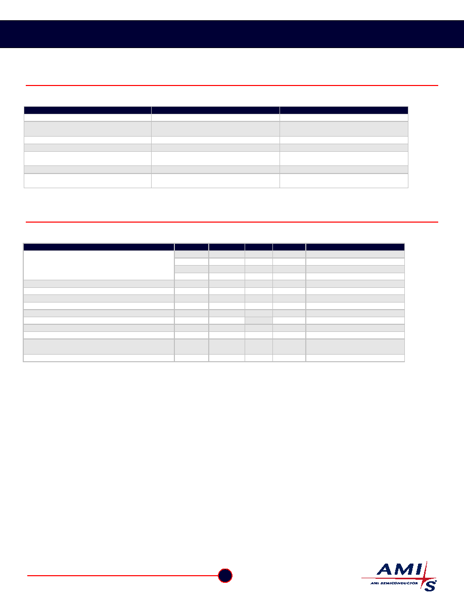
| 型號: | AMIS-710616-AS |
| 廠商: | ON SEMICONDUCTOR |
| 元件分類: | 圖像傳感器 |
| 英文描述: | IMAGE SENSOR-CMOS, 3V |
| 文件頁數(shù): | 12/19頁 |
| 文件大小: | 954K |
| 代理商: | AMIS-710616-AS |
AMIS-710616-AS: CIS PCB
Data Sheet
Product Specification
4.0 Physical Outline
Table 4-1: Physical Outline
Item
Specification
Note
Image sensors
AMIS-720639
See referenced image sensor data sheet
PCB stiffner board
PCB stiffner board size
355.6mm x 41.3mm x 6.35mm
Sensor PCB
Size
≈165.1mm x 21.4mm x 1.62mm
Two PCBs mounted on the stiffner
Data output
Eight analog video outputs
Sensor board connectors
Two I/O connectors
MOLEX 52610-1590
Used to connect to their respective output
amplifiers
Amplifier PCB board
Size
≈ 291.3mm x 76.2mm x 1.6mm
Amplifier board’s four connectors
Two inputs: MOLEX 52207-1950
Two outputs: ERNI-594083
Mounted are eight output amplifiers for each
of the video lines from the sensor boards
5.0 Recommended Operating Conditions (25
°C)
Table 5-1: Recommended Operating Conditions at 25
°C
Item
Symbol
Min.
Typ.
Max.
Units
VDD
4.5
5.0
5.5
V
IDD
135
150
165
ma
VSS
|-5.0|
|-5.5|
V
Power supply
ISS
45
60
ma
Video output levels
Vpavg
(1)
3.0
V
Video saturation output
VSATA
(2)
5.5
V
Video line saturation output
VSATV
(2)
1.2
V
Input voltage at digital high (input clocks, SP and CP)
VIH
VDD-1.0
VDD-.5
VDD+0.3
V
Input voltage at digital low (input clocks SP and CP)
VIL
0
0.8
V
Clock frequency
Freq
(3)
5.0
6.0
MHz
Clock pulse high duty cycle
Duty
(4)
25
75
%
Clock high duration
TPW
(3)(5)
83.3
100
Ns, at 50 percent duty
Integration time
Tint
192
s/line
160
s/line
Typical, tested @ 5.0MHz clock
Minimum, tested @ 6.0MHz clock
Operating temperature
Top
(6)
25
50
°C
Notes:
(1)
Vpavg is a symbol representing the average value of every pixel in the complete line scan. Vp(n) is the pixel amplitude of the nth pixel in a line scan. This
measurement is taken with the image array under a uniform light exposure. The typical output is specified with a uniform input light exposure of 0.5
J/cm2 from a
blue Led light source.
(2)
Two saturated video output levels are specified. One is at the video signal’s output amplifier, VSATA, and the other is at the input of the amplifier. In almost all
applications, because the integration time is usually too short, there is not enough exposure time to saturate the array sensors. Accordingly, each output amplifier
is fixed with a gain of
4.5.
(3)
Freq is generally fixed for any application for the following reasons: One is the exposure time. With a given light power, the exposure time of the sensor can be
related to the clock frequency. The second is the shape of the video output pulse. Because the output video is in pulse charge packets, the signals are processed
on the output video line of the sensors. Hence, the signal shape depends greatly upon the amplifier configurations. Please refer to the referenced AMIS-720639
data sheet. It has some brief outline application notes. Under Note 6 on Page 6, there is a discussion about video pulse shapes. On Page 8, 9 and 10 there are
discussions on the three types of signal output stages.
(4)
Duty is the ratio of the clock’s pulse width over its pulse period. Because the video pixel output resets during the clock pulse’s high period and because the reset
requires a finite resetting time, it is recommended to operate the clock duty cycle within the following limits. See the referenced data sheet in Note 3, above.
Noting that the larger the duty, the less the signal amplitude, while too short of a clock pulse will not provide enough video reset time and leaves residual charges,
the recommended duty is 25 percent for frequencies less than 5MHz and 50 percent for frequencies greater than 5MHz.
(5)
Tint is determined by the time interval between two start pulses, (SP). Hence, if the SP is generated from a clock count down circuit, it will be directly proportional
to the clock frequency and it will be synchronous with the clock frequency. The longest integration time is determined by the degree of leakage current degradation
that can be tolerated by the system. A 10ms maximum is a typical rule-of-thumb. An experienced CIS user can use his discretion and determine the desired
tolerance level for the given system.
(6)
Top is a conservative engineering estimate. It is based on measurements of similar CIS modules and simple bench top tests, using heat guns and freeze sprays.
These will be re-measured during the pilot production under the standard QA practices that are under the control of ISO 9000.
2
AMI Semiconductor – July 06, M-20595-001
www.amis.com
相關PDF資料 |
PDF描述 |
|---|---|
| AMMC-6345-W10 | 20000 MHz - 45000 MHz RF/MICROWAVE WIDE BAND MEDIUM POWER AMPLIFIER |
| AMMC-6345-W50 | 20000 MHz - 45000 MHz RF/MICROWAVE WIDE BAND MEDIUM POWER AMPLIFIER |
| AMMP-5620-BLKG | 6000 MHz - 20000 MHz RF/MICROWAVE WIDE BAND LOW POWER AMPLIFIER |
| AMMP-5620-TR2G | 6000 MHz - 20000 MHz RF/MICROWAVE WIDE BAND LOW POWER AMPLIFIER |
| AMMP-6222-TR2G | 7000 MHz - 21000 MHz RF/MICROWAVE WIDE BAND LOW POWER AMPLIFIER |
相關代理商/技術參數(shù) |
參數(shù)描述 |
|---|---|
| AMIS-710625 | 制造商:AMI 制造商全稱:AMI 功能描述:600pdi CIS Module |
| AMIS-710625-A6 | 制造商:AMI 制造商全稱:AMI 功能描述:600pdi CIS Module |
| AMIS-710627 | 制造商:AMI 制造商全稱:AMI 功能描述:600dpi CIS Modules |
| AMIS-710627-A4 | 制造商:AMI 制造商全稱:AMI 功能描述:600dpi CIS Modules |
| AMIS-710628-A4 | 制造商:AMI 制造商全稱:AMI 功能描述:600dpi CIS Modules |
發(fā)布緊急采購,3分鐘左右您將得到回復。