- 您現(xiàn)在的位置:買賣IC網(wǎng) > PDF目錄378405 > AND8066D (ON SEMICONDUCTOR) Interfacing with ECLinPS PDF資料下載
參數(shù)資料
| 型號: | AND8066D |
| 廠商: | ON SEMICONDUCTOR |
| 英文描述: | Interfacing with ECLinPS |
| 中文描述: | 接口與業(yè)界的EClinPS |
| 文件頁數(shù): | 5/8頁 |
| 文件大小: | 72K |
| 代理商: | AND8066D |
AND8066/D
http://onsemi.com
5
V
in
, (RELATIVE TO V
CC
)
V
in
, (RELATIVE TO V
CC
)
V
o
,
C
V
o
,
C
–1.2
–1.8
–0.8
–1.6
–1.4
–1.0
–1.2
–1.8
–0.8
–1.6
–1.4
–1.0
–2.0
–1.4
–1.6
–1.8
–1.2
–0.8
–1.0
–2.0
–1.4
–1.6
–1.8
–1.2
–0.8
–1.0
85
°
C
25
°
C
–30
°
C
70
°
C
25
°
C
0
°
C
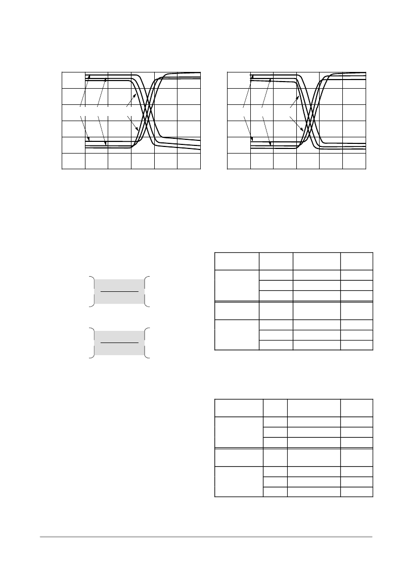
Figure 15. 10K Series Vin vs. Vout Transfer Curves
Figure 16. 10KH Series Vin vs. Vout Transfer Curves
The difference in the DC behavior of the inputs and outputs
of the two different standards necessitates caution when
mixing the two technologies in single–ended designs. Output
levels become critical to the receiver when the V
OH
minimum,
V
OHA
, drives into the receiver as the V
IH
minimum. Levels are
also critical when the driver V
OL
maximum, V
OLA
, drives into
the receiver as the V
IL
maximum.
Figure 17. Single–Ended Noise Margin
V
OH(max)
V
OH(min)
V
OHA
V
IH(max)
V
IH(min)
V
OL(max)
V
OLA
V
OL(min)
V
IL(max)
V
IH(min)
Noise margin quantifies the susceptibility of a driver and
receiver interface to any non–signal voltage levels and
therefore risking false switching. Two measurements –
NOISE MARGIN HIGH and NOISE MARGIN LOW –
describe the false switching risk across temperature as
follows:
NOISE MARGIN
(HIGH)
= V
OH(min)
– V
IH(min)
NOISE MARGIN
(LOW)
= V
OL(max)
– V
IL(max)
An MC10EP16DT, operating in LVPECL mode with 3.3 V
on V
CC
and 0.0 V on V
EE
, interfaced to an MC10EP16DT
receiver, single–ended, has a noise margin at the specification
ambient temperature shown in Table 1. Notice the safety
margin levels are positive for NOISE MARGIN HIGH
indicating the driver exceeds the receiver’s requirement for a
minimum and the delta is positive. For a NOISE MARGIN
LOW, the driver must be below the receiver’s maximum and
the delta is negative.
Table 1. Noise Margins: MC10EP16DT Interfaced to
an MC10EP16DT Receiver
10 to 10 Noise
Margin HIGH
Temp.
V
OH(min)
–
V
IH(min)
Delta
(mV)
–40
°
C
2165 – 2090
75
25
°
C
2230 – 2155
75
85
°
C
2290 – 2215
75
10 to 10 Noise
Margin LOW
Temp.
V
OL(max)
–
V
IL(max)
Delta
(mV)
–40
°
C
1615 – 1690
–40
25
°
C
1680 – 1755
–75
85
°
C
1740 – 1810
–70
When a 10 Series device drives a 100 Series device
single–ended, the noise margins become a risk factor requiring
careful evaluation as indicated in Table 2.
Table 2. Noise Margins: MC10EP16DT Interfaced to
an MC100EP16DT Receiver
10 to 100 Noise
Margin HIGH
Temp.
V
OH(min)
– V
IH(min)
Delta
(mV)
–40
°
C
2165 – 2075
90
25
°
C
2230 – 2075
155
85
°
C
2290 – 2075
215
10 to 100 Noise
Margin LOW
Temp.
V
OL(max)
– V
IL(max)
Delta
(mV)
–40
°
C
1615 – 1675
–60
25
°
C
1680 – 1675
5
85
°
C
1740 – 1675
65
相關PDF資料 |
PDF描述 |
|---|---|
| AND8067 | NL27WZ04 Dual Gate Inverter Oscillator Increases the Brightness of LEDs While Reducing Power Consumption |
| AND8079 | A Low Cost DDR Memory Power Supply Using the NCP1571 Synchronous Buck Converter and a LM358 Based Linear Voltage Regulator |
| AND8079D | A Low Cost DDR Memory Power Supply Using the NCP1571 Synchronous Buck Converter and a LM358 Based Linear Voltage Regulator |
| AND8085 | An Introduction to FST |
| AND8085D | An Introduction to FST |
相關代理商/技術(shù)參數(shù) |
參數(shù)描述 |
|---|---|
| AND8067 | 制造商:ONSEMI 制造商全稱:ON Semiconductor 功能描述:NL27WZ04 Dual Gate Inverter Oscillator Increases the Brightness of LEDs While Reducing Power Consumption |
| AND8079 | 制造商:ONSEMI 制造商全稱:ON Semiconductor 功能描述:A Low Cost DDR Memory Power Supply Using the NCP1571 Synchronous Buck Converter and a LM358 Based Linear Voltage Regulator |
| AND8079D | 制造商:ONSEMI 制造商全稱:ON Semiconductor 功能描述:A Low Cost DDR Memory Power Supply Using the NCP1571 Synchronous Buck Converter and a LM358 Based Linear Voltage Regulator |
| AND8085 | 制造商:ONSEMI 制造商全稱:ON Semiconductor 功能描述:An Introduction to FST |
| AND8085D | 制造商:ONSEMI 制造商全稱:ON Semiconductor 功能描述:An Introduction to FST |
發(fā)布緊急采購,3分鐘左右您將得到回復。