- 您現(xiàn)在的位置:買賣IC網(wǎng) > PDF目錄378412 > BF909 (NXP Semiconductors N.V.) N-channel dual-gate MOSFET PDF資料下載
參數(shù)資料
| 型號(hào): | BF909 |
| 廠商: | NXP Semiconductors N.V. |
| 元件分類: | 功率晶體管 |
| 英文描述: | N-channel dual-gate MOSFET |
| 封裝: | BF909<SOT143B (SOT143B)|<<http://www.nxp.com/packages/SOT143B.html<1<week 47, 2002,;BF909<SOT143B (SOT143B)|<<http://www.nxp.com/packages/SOT143B.html<1<week 47, 20 |
| 文件頁數(shù): | 6/12頁 |
| 文件大小: | 320K |
| 代理商: | BF909 |
NXP
Semiconductors
Product specification
N-channel dual gate MOS-FETs
BF909; BF909R
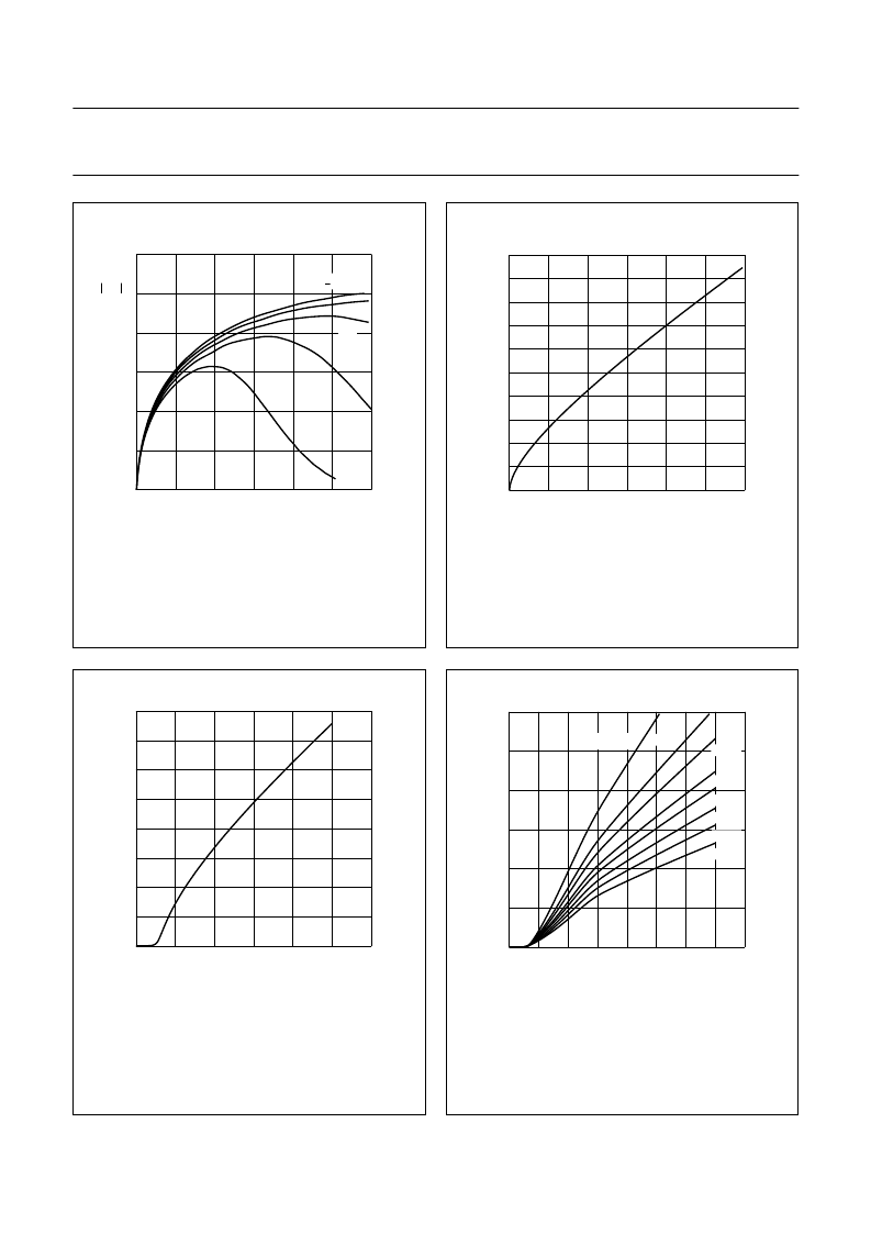
Fig.8
Forward transfer admittance as a
function of drain current; typical values.
V
DS
= 5 V.
T
j
= 25
°
C.
handbook, halfpage
0
40
20
0
10
20
30
MLB940
yfs
(mS)
ID
3.5 V
3 V
2.5 V
2 V
VG2 S
Fig.9
Drain current as a function of gate 1 current;
typical values.
V
DS
= 5 V; V
G2-S
= 4 V.
T
j
= 25
°
C.
handbook, halfpage
(mA)
0
20
40
60
0
20
15
10
5
IG1
μ
A)
Fig.10 Drain current as a function of gate 1
supply voltage (= V
GG
); typical values;
see Fig.18.
V
DS
= 5 V; V
G2-S
= 4 V.
R
G1
= 120 k
(connected to V
GG
); T
j
= 25
°
C.
handbook, halfpage
ID
(mA)
0
2
4
6
12
4
0
8
MLB942
VGG
Fig.11 Drain current as a function of gate 1
(= V
GG
) and drain supply voltage;
typical values; see Fig.18.
V
G2-S
= 4 V.
R
G1
connected to V
GG
; T
j
= 25
°
C.
handbook, halfpage
0
20
10
0
2
4
8
MLB943
6
VGG
DS
ID
(mA)
RG1
68 k
82 k
100 k
120 k
150 k
180 k
220 k
Rev. 02 - 19 November 2007
6 of 12
發(fā)布緊急采購,3分鐘左右您將得到回復(fù)。