- 您現(xiàn)在的位置:買賣IC網(wǎng) > PDF目錄373025 > BR211SM (NXP Semiconductors N.V.) Breakover diodes PDF資料下載
參數(shù)資料
| 型號: | BR211SM |
| 廠商: | NXP Semiconductors N.V. |
| 英文描述: | Breakover diodes |
| 中文描述: | 擊穿二極管 |
| 文件頁數(shù): | 1/6頁 |
| 文件大?。?/td> | 32K |
| 代理商: | BR211SM |
Philips Semiconductors
Preliminary specification
Breakover diodes
BR211SM series
GENERAL DESCRIPTION
QUICK REFERENCE DATA
A range of bidirectional, breakover
diodes in a two terminal, surface
mounting, plastic envelope. These
devices feature controlled breakover
voltage and high holding current
together with high peak current
handling
capability.
application is transient overvoltage
protection
in
telecommunications
equipment.
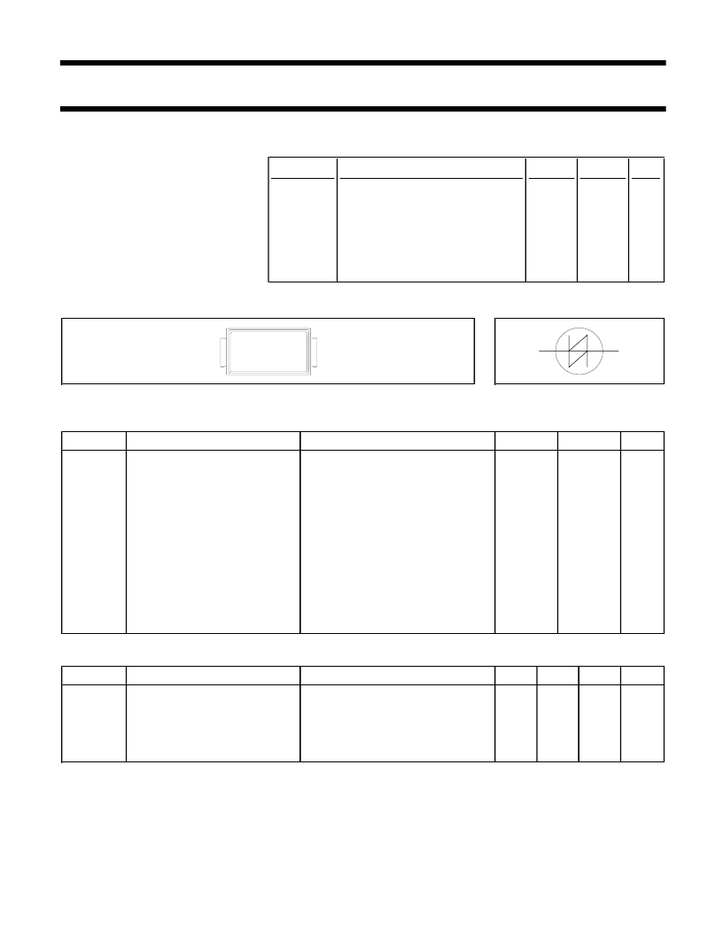
SYMBOL
PARAMETER
MIN.
MAX.
UNIT
BR211SM-140 to BR211SM-280
Breakover voltage
Holding current
Non-repetitive peak current
V
(BO)
I
H
I
TSM
140
150
-
280
-
40
V
mA
A
Typical
OUTLINE - SOD106
SYMBOL
LIMITING VALUES
Limiting values in accordance with the Absolute Maximum System (IEC 134).
SYMBOL
PARAMETER
V
D
Continuous voltage
CONDITIONS
MIN.
-
MAX.
75% of
V
(BO)typ
UNIT
V
I
TSM1
Non repetitive peak current
10/320
μ
s impulse equivalent to
10/700
μ
s, 1.6 kV voltage impulse
(CCITT K17)
half sine wave; t = 10 ms;
T
= 70 C prior to surge
t
p
= 10 ms
t
p
= 10
μ
s
-
A
I
TSM2
Non repetitive on-state current
-
15
A
I
2
t
dI
T
/dt
I
2
t for fusing
Rate of rise of on-state current
after V
turn-on
Continuous dissipation
Peak dissipation
Storage temperature
Operating ambient temperature off-state
Overload junction temperature
-
-
1.1
50
A
2
s
A/
μ
s
P
tot
P
TM
T
stg
T
a
T
vj
T
= 25C
t
p
= 1 ms; T
a
= 25C
-
-
1.2
50
150
70
150
W
W
C
C
C
- 40
-
-
on-state
THERMAL RESISTANCES
SYMBOL
PARAMETER
R
th j-sp
Thermal resistance junction to
solder point
R
th j-a
Thermal resistance junction to
ambient
Z
th j-a
Thermal impedance junction to
ambient
CONDITIONS
MIN.
-
TYP.
-
MAX.
12
UNIT
K/W
pcb mounted; minimum footprint
-
100
-
K/W
t
p
= 1 ms
-
2.62
-
K/W
August 1996
1
Rev 1.100
相關(guān)PDF資料 |
PDF描述 |
|---|---|
| BR211SM-140 | Breakover diodes |
| BR211SM-160 | MOSFET N-CH 500V 8A TO-220 |
| BR211SM-180 | Breakover diodes |
| BR211SM-200 | Breakover diodes |
| BR211SM-220 | Breakover diodes |
相關(guān)代理商/技術(shù)參數(shù) |
參數(shù)描述 |
|---|---|
| BR211SM-140 | 制造商:PHILIPS 制造商全稱:NXP Semiconductors 功能描述:Breakover diodes |
| BR211SM-160 | 制造商:PHILIPS 制造商全稱:NXP Semiconductors 功能描述:Breakover diodes |
| BR211SM-180 | 制造商:PHILIPS 制造商全稱:NXP Semiconductors 功能描述:Breakover diodes |
| BR211SM-200 | 制造商:PHILIPS 制造商全稱:NXP Semiconductors 功能描述:Breakover diodes |
| BR211SM-220 | 制造商:PHILIPS 制造商全稱:NXP Semiconductors 功能描述:Breakover diodes |
發(fā)布緊急采購,3分鐘左右您將得到回復(fù)。