- 您現(xiàn)在的位置:買賣IC網(wǎng) > PDF目錄366891 > CR16MCS9VJE7Y Microcontroller PDF資料下載
參數(shù)資料
| 型號: | CR16MCS9VJE7Y |
| 英文描述: | Microcontroller |
| 中文描述: | 微控制器 |
| 文件頁數(shù): | 122/157頁 |
| 文件大小: | 1256K |
| 代理商: | CR16MCS9VJE7Y |
第1頁第2頁第3頁第4頁第5頁第6頁第7頁第8頁第9頁第10頁第11頁第12頁第13頁第14頁第15頁第16頁第17頁第18頁第19頁第20頁第21頁第22頁第23頁第24頁第25頁第26頁第27頁第28頁第29頁第30頁第31頁第32頁第33頁第34頁第35頁第36頁第37頁第38頁第39頁第40頁第41頁第42頁第43頁第44頁第45頁第46頁第47頁第48頁第49頁第50頁第51頁第52頁第53頁第54頁第55頁第56頁第57頁第58頁第59頁第60頁第61頁第62頁第63頁第64頁第65頁第66頁第67頁第68頁第69頁第70頁第71頁第72頁第73頁第74頁第75頁第76頁第77頁第78頁第79頁第80頁第81頁第82頁第83頁第84頁第85頁第86頁第87頁第88頁第89頁第90頁第91頁第92頁第93頁第94頁第95頁第96頁第97頁第98頁第99頁第100頁第101頁第102頁第103頁第104頁第105頁第106頁第107頁第108頁第109頁第110頁第111頁第112頁第113頁第114頁第115頁第116頁第117頁第118頁第119頁第120頁第121頁當前第122頁第123頁第124頁第125頁第126頁第127頁第128頁第129頁第130頁第131頁第132頁第133頁第134頁第135頁第136頁第137頁第138頁第139頁第140頁第141頁第142頁第143頁第144頁第145頁第146頁第147頁第148頁第149頁第150頁第151頁第152頁第153頁第154頁第155頁第156頁第157頁

www.national.com
122
000 = 1 A/D Converter clock cycle
001 = 2 A/D Converter clock cycles
010 = 4 A/D Converter clock cycles
011 = 8 A/D Converter clock cycles
100 = 16 A/D Converter clock cycles
101 = 32 A/D Converter clock cycles
110 = 64 A/D Converter clock cycles
111 = reserved
Power Down Enable.
c
ontrols the condition
when the ADC is powered down. When
PWREN is cleared (0), the ADC powers down
upon reset. When PWREN is set (1), the ADC
powers down when the ADCEN bit is low.
PWREN
22.2.5
The four ADC Data Registers (ADDATA0 through ADDATA3)
are byte-wide, read/write registers that hold the conversion
results, which are stored sequentially starting with ADDATA0
and ending with ADDATA3. The results held in these regis-
ters are valid only after the ADCST.EOC flag is set. Upon re-
set, the contents of these registers are undefined.
The value read from a data register is a linear mapping of the
analog input voltage to an 8-bit value. The value 00 hex rep-
resents 0.0 volts and the value FF hex represents the refer-
ence voltage, VREF.
22.3
A/D CONVERTER PROGRAMMING
The software should set the A/D Converter configuration be-
fore it enables the A/D Converter module. The configuration
consists of the following settings:
— ADC clock rate: ADCCNT3.CDIV
— Sampling delay: ADCCNT3.DELAY
— Interrupt enable (if required): ADCCNT1.INTE
The ADC clock is created by scaling down the system clock.
The fastest allowable clock for the A/D Converter is 2 MHz.
Therefore, for the fastest possible operation of the A/D Con-
verter, use the smallest available divide-by factor that results
in a clock frequency of 1 MHz or lower. The available divide-
by factors are 1, 2, 4, 8, 16, and 32.
For example, if the system clock is 10 MHz, use a divide-by
factor of 16. In that case, the A/D Converter clock frequency
is 625 kHz, the clock period is 1.6 microseconds, and the A/
ADC Data Registers (ADDATA0-ADDATA3)
D conversion time is 16 microseconds (ten clock A/D Con-
verter clock cycles).
The programmable sampling time delay should be made
small for faster operation, but large enough to allow the input
voltage to settle. The internal resistance and capacitance of
the A/D Converter, together with the source resistance of the
device that drives the A/D input determine the charge-up time
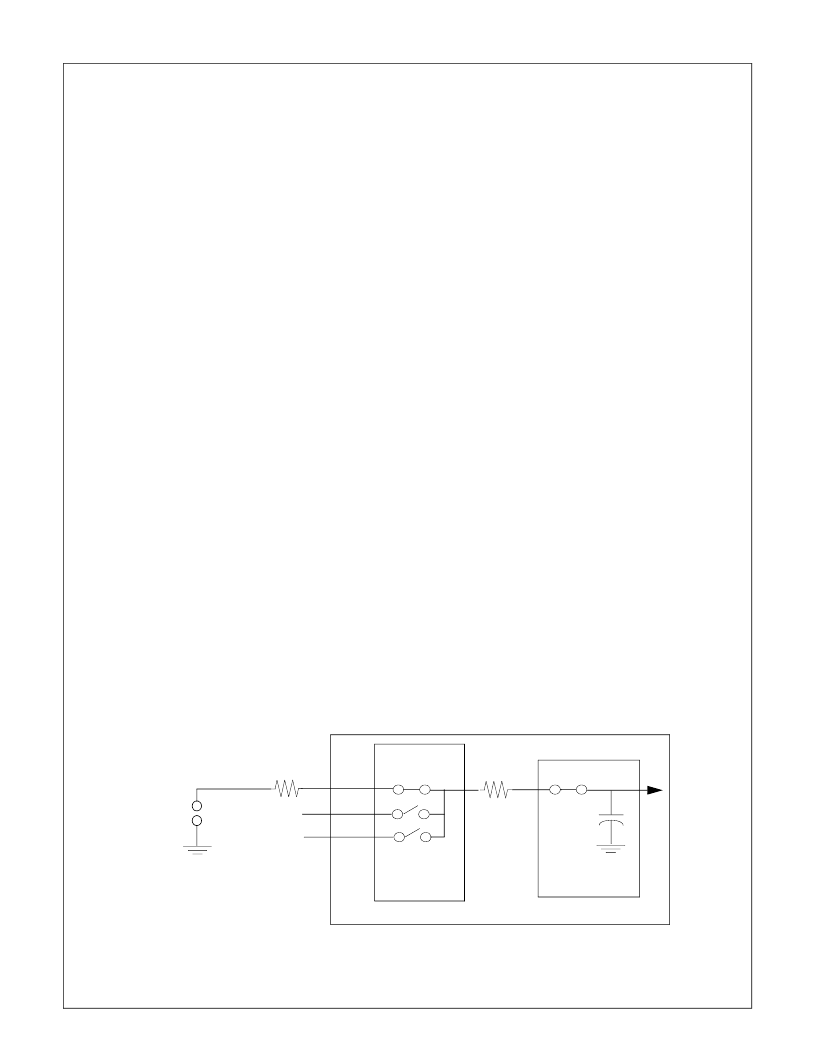
required for the voltage to settle. Figure 75 shows a schemat-
ic of the charge-up circuit. For the values of RAIN and CAIN,
see Section 25.0.
Interrupts or polling can be used to read the A/D Converter
results. For interrupts, the A/D Converter interrupt must be
enabled by setting the ADCCNT1.INTE bit. The interrupt is
cleared automatically when any one of the data registers
(ADDATA0-ADDATA3) is read. For polling, the software
reads the ADCST.EOC bit to determine whether the conver-
sion sequence is completed.
Once the A/D Converter configuration has been set up, the
software can use the following procedure to perform an A/D
conversion sequence:
1. Enable the A/D Converter by setting the ADCCNT1.AD-
CEN bit and wait 30 ms before performing any conver-
sion.
2. Select the operating mode and channel by writing to the
SCAN, CONT, and CHANNEL fields of the ADCCNT2
register. At the same time, start the conversion by setting
the START bit in the same register.
3. Wait until the conversion is finished, either by polling or
using the A/D Converter interrupt.
4. Read the conversion results from the data registers,
ADDATA0 through ADDATA3 (or just ADDATA0 in the
single-channel, single-conversion mode).
5. In the continuous conversion modes, repeat Step 3 and
Step 4 for as long as samples are needed. Then stop the
A/D Converter by clearing either the START bit
(ADCCNT2.START) or the A/D Converter enable bit
(ADCCNT1.ADCEN).
To minimize power consumption, the A/D Converter should
be disabled when it is not needed, especially before entering
a Power Save mode.
Figure 75.
Sample-and-Hold Charge-Up Schematic
A/D Converter
Analog
Multiplexer
Sample &
Hold
R
AIN
C
AIN
Input
signal
R
SOURCE
相關(guān)PDF資料 |
PDF描述 |
|---|---|
| CR16MCS9VJE8 | Microcontroller |
| CR16MCS9VJE8Y | Microcontroller |
| CR16MCT5VJE7Y | Microcontroller |
| CR16HCS5VJE8 | Microcontroller |
| CR16HCS9VJE7Y | Microcontroller |
相關(guān)代理商/技術(shù)參數(shù) |
參數(shù)描述 |
|---|---|
| CR16MCS9VJE8 | 功能描述:16位微控制器 - MCU RoHS:否 制造商:Texas Instruments 核心:RISC 處理器系列:MSP430FR572x 數(shù)據(jù)總線寬度:16 bit 最大時鐘頻率:24 MHz 程序存儲器大小:8 KB 數(shù)據(jù) RAM 大小:1 KB 片上 ADC:Yes 工作電源電壓:2 V to 3.6 V 工作溫度范圍:- 40 C to + 85 C 封裝 / 箱體:VQFN-40 安裝風格:SMD/SMT |
| CR16MCS9VJE8/NOPB | 功能描述:16位微控制器 - MCU RoHS:否 制造商:Texas Instruments 核心:RISC 處理器系列:MSP430FR572x 數(shù)據(jù)總線寬度:16 bit 最大時鐘頻率:24 MHz 程序存儲器大小:8 KB 數(shù)據(jù) RAM 大小:1 KB 片上 ADC:Yes 工作電源電壓:2 V to 3.6 V 工作溫度范圍:- 40 C to + 85 C 封裝 / 箱體:VQFN-40 安裝風格:SMD/SMT |
| CR16MCS9VJE80 | 制造商:NSC 制造商全稱:National Semiconductor 功能描述:Family of 16-bit CAN-enabled CompactRISC Microcontrollers |
| CR16MCS9VJE81 | 制造商:NSC 制造商全稱:National Semiconductor 功能描述:Family of 16-bit CAN-enabled CompactRISC Microcontrollers |
| CR16MCS9VJE82 | 制造商:NSC 制造商全稱:National Semiconductor 功能描述:Family of 16-bit CAN-enabled CompactRISC Microcontrollers |
發(fā)布緊急采購,3分鐘左右您將得到回復。