- 您現(xiàn)在的位置:買賣IC網(wǎng) > PDF目錄374166 > CS51311GDR14 (ZF Electronics Corporation) Synchronous CPU Buck Controller for 12V and 5V Applications PDF資料下載
參數(shù)資料
| 型號: | CS51311GDR14 |
| 廠商: | ZF Electronics Corporation |
| 英文描述: | Synchronous CPU Buck Controller for 12V and 5V Applications |
| 中文描述: | 同步降壓控制器的CPU為12V和5V的應(yīng)用 |
| 文件頁數(shù): | 2/19頁 |
| 文件大?。?/td> | 239K |
| 代理商: | CS51311GDR14 |
2
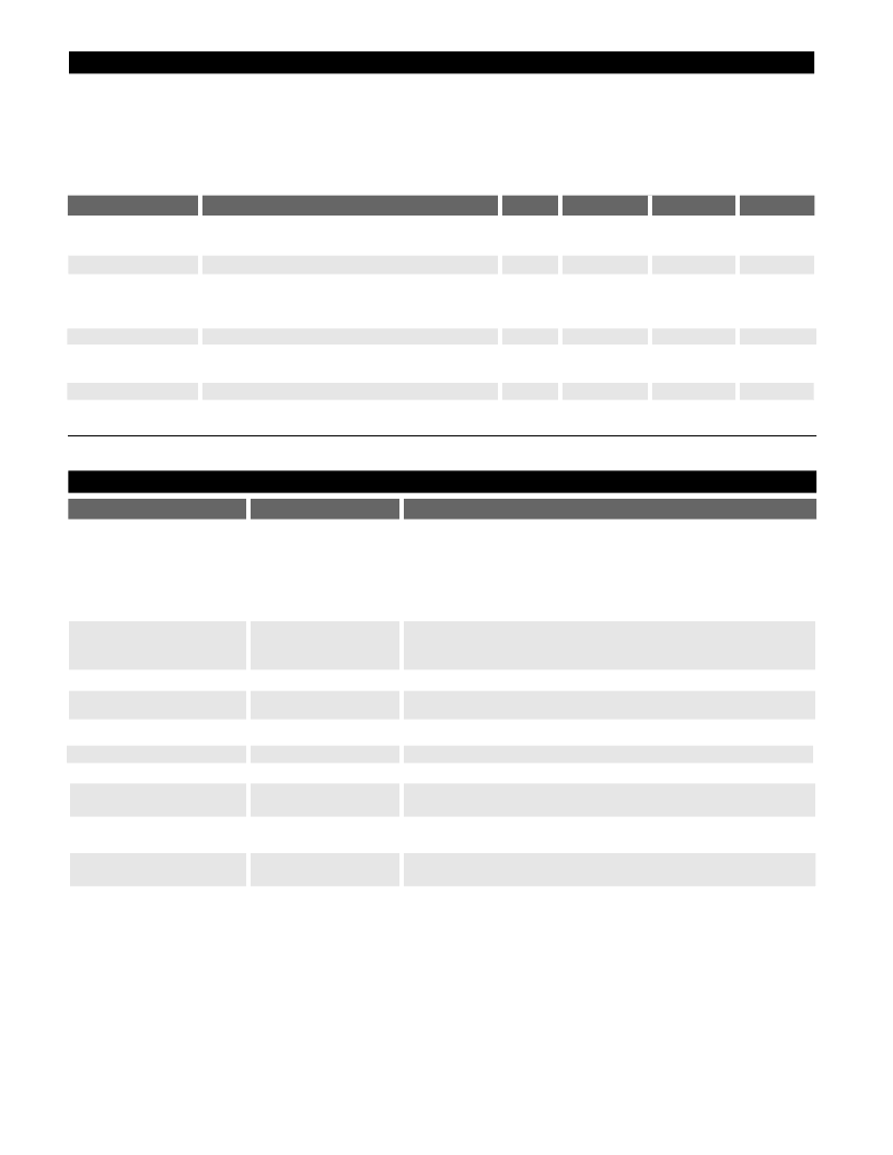
Package Pin Description
PACKAGE PIN #
PIN SYMBOL
FUNCTION
Absolute Maximum Ratings
Pin Symbol
Pin Name
V
MAX
V
MIN
I
SOURCE
I
SINK
C
Operating Junction Temperature, T
J
. . . . . . . . . . . . . . . . . . . . . . . . . . . . . . . . . . . . . . . . . . . . . . . . . . . . . . . . . . . . . . . 150°C
Lead Temperature Soldering
Reflow (SMD styles only) . . . . . . . . . . . . . . . . . . . . . . . . . . . . . . . . . . . . . . . . . . .60 sec. max above 183°C, 230°C peak
Storage Temperature Range, T
S
. . . . . . . . . . . . . . . . . . . . . . . . . . . . . . . . . . . . . . . . . . . . . . . . . . . . . . . . . . . . . -65° to 150°C
ESD Susceptibility . . . . . . . . . . . . . . . . . . . . . . . . . . . . . . . . . . . . . . . . . . . . . . . . . . . . . . . . . . . . . . . . . . . . . . . . . . . . . . . . 2kV
V
CC
IC Power Input
16V
-0.3V
N/A
1.5 APeak
200mA DC
5mA
1mA
COMP
V
FB
, V
OUT
, V
ID0-4
Compensation Pin
Voltage Feedback Input, Output
Voltage Sense Pin, Voltage
ID DAC Inputs
Off-Time Pin
High-Side, Low-Side FET Drivers
6V
6V
-0.3V
-0.3V
1mA
1mA
C
OFF
GATE(H), GATE(L)
6V
16V
-0.3V
-0.3V DC
1mA
1.5APeak
200mA DC
1mA
1.5A Peak
200mA DC
50mA
1.5A Peak
200mA DC
30mA
N/A
PWRGD
Gnd
Power-Good Output
Ground
6V
0V
-0.3V
0V
1,2,3,4,5
V
IDO
– V
ID4
Voltage ID DAC inputs. These pins are internally pulled up to
5.65V if left open. V
ID4
selects the DAC range. When V
ID4
is
high (logic one), the Error Amp reference range is 2.125V to
3.525V with 100mV increments. When V
ID4
is low (logic zero),
the Error amp reference voltage is 1.325V to 2.075V with 50mV
increments.
Error amp inverting input, PWM comparator non-inverting
input, current limit comparator non-inverting input, PWRGD
comparator input.
Current limit comparator inverting input.
Input power supply pin for the internal circuitry.
Decouple with filter capacitor to Gnd.
High side switch FET driver pin .
Ground pin.
Low side synchronous FET driver pin.
Power-Good Output. Open collector output drives low when
V
FB
is out of regulation.
Off-Time Capacitor Pin. A capacitor from this pin to Gnd sets
the off time for the regulator
Error amp output. PWM comparator inverting input.
A capacitor on this pin provides error amp compensation.
6
V
FB
7
8
V
OUT
V
CC
9
10
11
12
GATE(H)
Gnd
GATE(L)
PWRGD
13
C
OFF
14
COMP
相關(guān)PDF資料 |
PDF描述 |
|---|---|
| CS51311 | Synchronous CPU Buck Controller for 12V and 5V Applications |
| CS51311GD14 | Synchronous CPU Buck Controller for 12V and 5V Applications |
| CS51312GDR16 | Synchronous CPU Buck Controller for 12V Only Applications |
| CS51312 | Synchronous CPU Buck Controller for 12V Only Applications |
| CS51312GD16 | Synchronous CPU Buck Controller for 12V Only Applications |
相關(guān)代理商/技術(shù)參數(shù) |
參數(shù)描述 |
|---|---|
| CS-51313D16 | 制造商:未知廠家 制造商全稱:未知廠家 功能描述:Current-Mode SMPS Controller |
| CS-51313DR16 | 制造商:未知廠家 制造商全稱:未知廠家 功能描述:Current-Mode SMPS Controller |
| CS51313GDR16 | 制造商:Rochester Electronics LLC 功能描述: 制造商:ON Semiconductor 功能描述: |
| CS-5132 | 制造商:未知廠家 制造商全稱:未知廠家 功能描述:Dual Output CPU Buck Controller |
| CS5132DW24 | 制造商:ON Semiconductor 功能描述: |
發(fā)布緊急采購,3分鐘左右您將得到回復(fù)。