- 您現(xiàn)在的位置:買(mǎi)賣(mài)IC網(wǎng) > PDF目錄295335 > CS5332GDW28 (ON SEMICONDUCTOR) 1.5 A SWITCHING CONTROLLER, 1000 kHz SWITCHING FREQ-MAX, PDSO28 PDF資料下載
參數(shù)資料
| 型號(hào): | CS5332GDW28 |
| 廠商: | ON SEMICONDUCTOR |
| 元件分類(lèi): | 穩(wěn)壓器 |
| 英文描述: | 1.5 A SWITCHING CONTROLLER, 1000 kHz SWITCHING FREQ-MAX, PDSO28 |
| 封裝: | SOP-28 |
| 文件頁(yè)數(shù): | 4/20頁(yè) |
| 文件大小: | 400K |
| 代理商: | CS5332GDW28 |
第1頁(yè)第2頁(yè)第3頁(yè)當(dāng)前第4頁(yè)第5頁(yè)第6頁(yè)第7頁(yè)第8頁(yè)第9頁(yè)第10頁(yè)第11頁(yè)第12頁(yè)第13頁(yè)第14頁(yè)第15頁(yè)第16頁(yè)第17頁(yè)第18頁(yè)第19頁(yè)第20頁(yè)

CS5332
http://onsemi.com
12
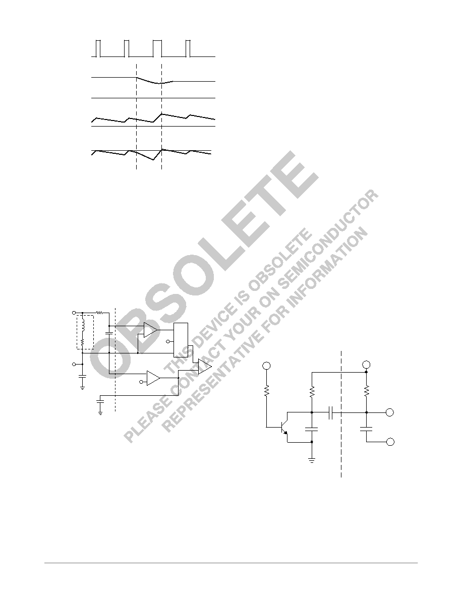
SWNODE
VFB (VOUT)
CSA Out
CSA Out + VFB
Figure 10. Open Loop Operation
COMP Offset
T1
T2
Inductive Current Sensing
For lossless sensing current can be sensed across the
inductor as shown in Figure 11. In the diagram, L is the
output inductance and RL is the inherent inductor resistance.
To compensate the current sense signal the values of R1 and
C1 are chosen so that L/RL = R1 × C1. If this criteria is met
the current sense signal will be the same shape as the
inductor current, the voltage signal at Cx will represent the
instantaneous value of inductor current and the circuit can be
analyzed as if a sense resistor of value RL was used as a sense
resistor (RS).
SWNODE
VOUT
DACOUT
COMP
VFB
CSREF
CSX
CSA
OFFSET
PWM-
COMP
E.A.
R1
C1
L
RL
+
Figure 11. Lossless Inductive Current Sensing with
Enhanced V2
When choosing or designing inductors for use with
inductive sensing, tolerances and temperature effects should
be considered. Cores with a low permeability material or a
large gap will usually have minimal inductance change with
temperature and load. Copper magnet wire has a
temperature coefficient of 0.39% per °C. The increase in
winding resistance at higher temperatures should be
considered when setting the ILIM threshold. If a more
accurate current sense is required than inductive sensing can
provide, current can be sensed through a resistor as shown
in Figure 9.
Current Sharing Accuracy
PCB traces that carry inductor current can be used as part
of the current sense resistance depending on where the
current sense signal is picked off. For accurate current
sharing, the current sense inputs should sense the current at
the same point for each phase and the connection to the
CSREF should be made so that no phase is favored. (In some
cases, especially with inductive sensing, resistance of the
pcb can be useful for increasing the current sense
resistance.) The total current sense resistance used for
calculations must include any pcb trace between the CS
inputs and the CSREF input that carries inductor current.
Current Sense Amplifier Input Mismatch and the value of
the current sense element will determine the accuracy of
current sharing between phases. The worst case Current
Sense Amplifier Input Mismatch is 5.0 mV and will typically
be within 3.0 mV. The difference in peak currents between
phases will be the CSA Input Mismatch divided by the current
sense resistance. If all current sense elements are of equal
resistance, a 3.0 mV mismatch with a 2.0 mΩ sense resistance
will produce a 1.5 A difference in current between phases.
Operation at > 50% Duty Cycle
For operation at duty cycles above 50% Enhanced V2
will exhibit subharmonic oscillation unless a compensation
ramp is added to each phase. A circuit like the one on the left
side of Figure 12 can be added to each current sense network
to implement slope compensation. The value of R1 can be
varied to adjust the ramp size.
Switch Node
CSX
CSREF
25 k
R1
.01 μF
1.0 nF
0.1 μF
3.0 k
GATE(L)X
Slope Comp
Circuit
Existing Current
Sense Circuit
MMBT2222LT1
Figure 12. External Slope Compensation Circuit
相關(guān)PDF資料 |
PDF描述 |
|---|---|
| CS600/L2 | 1 CHANNEL LOGIC OUTPUT OPTOCOUPLER |
| CSBLA384KECE-B0 | CERAMIC RESONATOR, 0.384 MHz |
| CSC5026-0102F | 16 CONTACT(S), COMBINATION LINE CONNECTOR, SOCKET |
| CSD10030 | ZERO RECOVERY RECTIFIER |
| CSD10030A | ZERO RECOVERY RECTIFIER |
相關(guān)代理商/技術(shù)參數(shù) |
參數(shù)描述 |
|---|---|
| CS5332GDWR28 | 功能描述:IC REG CTRLR BUCK PWM 28-SOIC RoHS:否 類(lèi)別:集成電路 (IC) >> PMIC - 穩(wěn)壓器 - DC DC 切換控制器 系列:- 標(biāo)準(zhǔn)包裝:4,000 系列:- PWM 型:電壓模式 輸出數(shù):1 頻率 - 最大:1.5MHz 占空比:66.7% 電源電壓:4.75 V ~ 5.25 V 降壓:是 升壓:無(wú) 回掃:無(wú) 反相:無(wú) 倍增器:無(wú) 除法器:無(wú) Cuk:無(wú) 隔離:無(wú) 工作溫度:-40°C ~ 85°C 封裝/外殼:40-VFQFN 裸露焊盤(pán) 包裝:帶卷 (TR) |
| CS5333 | 制造商:CIRRUS 制造商全稱(chēng):Cirrus Logic 功能描述:24-Bit, 96 kHz Stereo A/D Converter |
| CS5333-BZ | 制造商:Rochester Electronics LLC 功能描述:- Bulk |
| CS5333-KZ | 制造商:CIRRUS 制造商全稱(chēng):Cirrus Logic 功能描述:24-Bit, 96 kHz Stereo A/D Converter |
| CS5333-KZR | 制造商:Cirrus Logic 功能描述: |
發(fā)布緊急采購(gòu),3分鐘左右您將得到回復(fù)。