- 您現(xiàn)在的位置:買賣IC網(wǎng) > PDF目錄170345 > CY38050V256-125BBI (CYPRESS SEMICONDUCTOR CORP) LOADABLE PLD, 10 ns, PBGA256 PDF資料下載
參數(shù)資料
| 型號(hào): | CY38050V256-125BBI |
| 廠商: | CYPRESS SEMICONDUCTOR CORP |
| 元件分類: | PLD |
| 英文描述: | LOADABLE PLD, 10 ns, PBGA256 |
| 封裝: | 17 X 17 MM, FBGA-256 |
| 文件頁數(shù): | 5/45頁 |
| 文件大小: | 720K |
| 代理商: | CY38050V256-125BBI |
第1頁第2頁第3頁第4頁當(dāng)前第5頁第6頁第7頁第8頁第9頁第10頁第11頁第12頁第13頁第14頁第15頁第16頁第17頁第18頁第19頁第20頁第21頁第22頁第23頁第24頁第25頁第26頁第27頁第28頁第29頁第30頁第31頁第32頁第33頁第34頁第35頁第36頁第37頁第38頁第39頁第40頁第41頁第42頁第43頁第44頁第45頁
Quantum38K ISR
CPLD Family
Document #: 38-03043 Rev. *G
Page 13 of 45
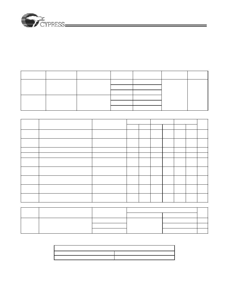
Maximum Ratings
(Above which the useful life may be impaired. For user guide-
lines, not tested.)
Storage Temperature .................................. –65
°C to +150°C
Soldering Temperature................................................. 220
°C
Ambient Temperature with
Power Applied............................................... –40
°C to +85°C
Junction Temperature .................................................. 135
°C
VCC to Ground Potential ...................................–0.5V to 4.6V
VCCIO to Ground Potential ................................–0.5V to 4.6V
DC Voltage Applied to Outputs in High-Z State –0.5V to 4.5V
DC Input voltage...............................................–0.5V to 4.5V
DC Current into Outputs ............................................ ±20 mA
Static Discharge Voltage
(per JEDEC EIA/JESD22-A114A) ............................ > 2001V
Latch-up Current..................................................... > 200 mA
Notes:
4.
The Voltage on any input or I/O pin cannot exceed the power pin during power-up.
5.
Input Leakage current is ±10
A for all the pins on all the Quantum38K package except the following pins in Quantum 38K100 packages: The input leakage
current spec for these pins in ±200
A.
6.
Not more than one output should be tested at a time. Duration of the short circuit should not exceed 1 second. VOUT = 0.5V has been chosen to avoid test
problems caused by tester ground degradation. Tested initially and after any design or process changes that may affect this parameter.
Operating Range[4]
Range
Ambient
Temperature
Junction
Temperature
Output
Condition
VCCIO
VCC
VCCJTAG/
VCCCNFG
Commercial
0
°C to +70°C
0
°C to +85°C
3.3V
3.3V ± 0.3V
3.3V ± 0.3V or
2.5V ± 0.2V
Same as
VCCIO
2.5V
2.5V ± 0.2V
1.8V
1.8 ± 0.15V
Industrial
–40
°C to +85°C
–40
°C to +100°C
3.3V
3.3V ± 0.3V
2.5V
2.5V ± 0.2V
1.8V
1.8 ± 0.15V
DC Characteristics
Parameter
Description
Test Conditions
VCCIO = 3.3V
VCCIO = 2.5V
VCCIO = 1.8V
Unit
Min.
Max.
Min.
Max.
Min.
Max.
VDRINT
Data Retention VCC Voltage
(config data may be lost below this)
1.5
V
VDRIO
Data Retention VCCIO Voltage
(config data may be lost below this)
1.2
V
IIX
[5]
Input Leakage Current
GND
≤ V
I ≤ 3.6V
–10
10
–10
10
–10
10
A
IOZ
Output Leakage Current
GND
≤ V
O ≤ VCCIO
–10
10
–10
10
–10
10
A
IOS
[6]
Output Short Circuit Current
VCCIO = Max., VOUT =
0.5V
–160
A
IBHL
Input Bus Hold LOW Sustaining
Current
VCC = Min., VPIN = VIL
+40
+30
+25
A
IBHH
Input Bus Hold HIGH Sustaining
Current
VCC = Min., VPIN = VIH
–40
–30
–25
A
IBHLO
Input Bus Hold LOW Overdrive
Current
VCC = Max.
+250
+200
+150
A
IBHHO
Input Bus Hold HIGH Overdrive
Current
VCC = Max.
–250
–200
–150
A
Parameter
Description
Device
VCC= 3.3 V/2.5V
Unit
Min.
Max
ICC0
Standby Current
38K30
20
mA
38K50
20
mA
38K100
30
mA
Quantum 38K100
Package
Pins
484-FBGA
B8, G9
相關(guān)PDF資料 |
PDF描述 |
|---|---|
| CY38050V484-125BBC | LOADABLE PLD, 10 ns, PBGA484 |
| CY38050V484-125BBI | LOADABLE PLD, 10 ns, PBGA484 |
| CY39030Z144-222BBC | LOADABLE PLD, 7 ns, PBGA144 |
| CY39030Z144-83BBC | LOADABLE PLD, 15 ns, PBGA144 |
| CY39030Z144-83BBI | LOADABLE PLD, 15 ns, PBGA144 |
相關(guān)代理商/技術(shù)參數(shù) |
參數(shù)描述 |
|---|---|
| CY38100V208-125NTI | 制造商:Cypress Semiconductor 功能描述:CPLD QUANTUM38K 144K GATES 1536 MCRCLLS IND 0.18UM 2.5V/3.3V - Bulk |
| CY3858-000 | 制造商:TE Connectivity 功能描述:2524F0524-1L/9-9-L016 - Cable Rools/Shrink Tubing |
| CY39 | 制造商:PLETRONICS 制造商全稱:Pletronics, Inc. 功能描述:Crystals |
| CY3900I | 功能描述:開發(fā)軟件 ISR Programming Kit RoHS:否 制造商:Atollic Inc. 產(chǎn)品:Compilers/Debuggers 用于:ARM7, ARM9, Cortex-A, Cortex-M, Cortex-R Processors |
| CY3900I_05 | 制造商:CYPRESS 制造商全稱:Cypress Semiconductor 功能描述:Delta39K⑩⁄Ultra37000⑩ ISR⑩ Programming Kits |
發(fā)布緊急采購,3分鐘左右您將得到回復(fù)。