- 您現(xiàn)在的位置:買賣IC網(wǎng) > PDF目錄170346 > CY62126DV30LL-70ZIT (CYPRESS SEMICONDUCTOR CORP) 64K X 16 STANDARD SRAM, 70 ns, PDSO44 PDF資料下載
參數(shù)資料
| 型號: | CY62126DV30LL-70ZIT |
| 廠商: | CYPRESS SEMICONDUCTOR CORP |
| 元件分類: | SRAM |
| 英文描述: | 64K X 16 STANDARD SRAM, 70 ns, PDSO44 |
| 封裝: | TSOP2-44 |
| 文件頁數(shù): | 1/13頁 |
| 文件大?。?/td> | 250K |
| 代理商: | CY62126DV30LL-70ZIT |
1-Mbit (64K x 16) Static RAM
CY62126DV30
MoBL
Cypress Semiconductor Corporation
3901 North First Street
San Jose
, CA 95134
408-943-2600
Document #: 38-05230 Rev. *G
Revised May 30, 2005
Features
Temperature Ranges
— Industrial: –40°C to 85°C
— Automotive: –40°C to 125°C
Very high speed: 45 ns
Wide voltage range: 2.2V to 3.6V
Pin compatible with CY62126BV
Ultra-low active power
— Typical active current: 0.85 mA @ f = 1 MHz
— Typical active current: 5 mA @ f = fMAX
Ultra-low standby power
Easy memory expansion with CE and OE features
Automatic power-down when deselected
Packages offered in a 48-ball FBGA, 56-lead QFN and
a 44-lead TSOP Type II
Also available in Lead-free packages
Functional Description[1]
The CY62126DV30 is a high-performance CMOS static RAM
organized as 64K words by 16 bits. This device features
advanced circuit design to provide ultra-low active current.
This is ideal for providing More Battery Life (MoBL) in
portable applications such as cellular telephones. The device
also has an automatic power-down feature that significantly
reduces power consumption by 90% when addresses are not
toggling. The device can be put into standby mode reducing
power consumption by more than 99% when deselected (CE
HIGH). The input/output pins (I/O0 through I/O15) are placed
in a high-impedance state when: deselected (CE HIGH),
outputs are disabled (OE HIGH), both Byte High Enable and
Byte Low Enable are disabled (BHE, BLE HIGH) or during a
write operation (CE LOW and WE LOW).
Writing to the device is accomplished by taking Chip Enable
(CE) and Write Enable (WE) inputs LOW. If Byte Low Enable
(BLE) is LOW, then data from I/O pins (I/O0 through I/O7), is
written into the location specified on the address pins (A0
through A15). If Byte High Enable (BHE) is LOW, then data
from I/O pins (I/O8 through I/O15) is written into the location
specified on the address pins (A0 through A15).
Reading from the device is accomplished by taking Chip
Enable (CE) and Output Enable (OE) LOW while forcing the
Write Enable (WE) HIGH. If Byte Low Enable (BLE) is LOW,
then data from the memory location specified by the address
pins will appear on I/O0 to I/O7. If Byte High Enable (BHE) is
LOW, then data from memory will appear on I/O8 to I/O15. See
the truth table at the back of this data sheet for a complete
description of read and write modes.
Note:
1. For best-practice recommendations, please refer to the Cypress application note “System Design Guidelines” on http://www.cypress.com.
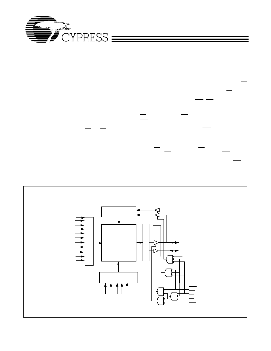
Logic Block Diagram
64K x 16
RAM Array
I/O0–I/O7
ROW
DECODER
A8
A7
A6
A5
A2
COLUMN DECODER
A
11
A
12
A
13
A
14
A
15
2048 x 512
SE
NSE
AMPS
DATA IN DRIVERS
OE
A4
A3
I/O8–I/O15
CE
WE
BLE
BHE
A0
A1
A9
A10
相關(guān)PDF資料 |
PDF描述 |
|---|---|
| CY62148L-100SC | 512K X 8 STANDARD SRAM, 100 ns, PDSO32 |
| CY74FCT158ATPC | FCT SERIES, QUAD 2 LINE TO 1 LINE MULTIPLEXER, INVERTED OUTPUT, PDIP16 |
| CY74FCT377ATQC | FCT SERIES, POSITIVE EDGE TRIGGERED D FLIP-FLOP, TRUE OUTPUT, PDSO20 |
| CY7B155-12LC | 16K X 16 STANDARD SRAM, 12 ns, CQCC52 |
| CY7B155-15JC | 16K X 16 STANDARD SRAM, 15 ns, PQCC52 |
相關(guān)代理商/技術(shù)參數(shù) |
參數(shù)描述 |
|---|---|
| CY62126DV30LL-70ZSI | 制造商:CYPRESS 制造商全稱:Cypress Semiconductor 功能描述:1-Mbit (64K x 16) Static RAM |
| CY62126DV30LL-70ZSXI | 制造商:CYPRESS 制造商全稱:Cypress Semiconductor 功能描述:1-Mbit (64K x 16) Static RAM |
| CY62126DV30LL-70ZXI | 制造商:Rochester Electronics LLC 功能描述: 制造商:Cypress Semiconductor 功能描述: |
| CY62126ESL | 制造商:CYPRESS 制造商全稱:Cypress Semiconductor 功能描述:1-Mbit (64K x 16) Static RAM |
| CY62126ESL_13 | 制造商:CYPRESS 制造商全稱:Cypress Semiconductor 功能描述:1-Mbit (64 K x 16) Static RAM |
發(fā)布緊急采購,3分鐘左右您將得到回復(fù)。