- 您現(xiàn)在的位置:買賣IC網(wǎng) > PDF目錄170346 > CY62126DV30LL-70ZIT (CYPRESS SEMICONDUCTOR CORP) 64K X 16 STANDARD SRAM, 70 ns, PDSO44 PDF資料下載
參數(shù)資料
| 型號(hào): | CY62126DV30LL-70ZIT |
| 廠商: | CYPRESS SEMICONDUCTOR CORP |
| 元件分類: | SRAM |
| 英文描述: | 64K X 16 STANDARD SRAM, 70 ns, PDSO44 |
| 封裝: | TSOP2-44 |
| 文件頁(yè)數(shù): | 10/13頁(yè) |
| 文件大小: | 250K |
| 代理商: | CY62126DV30LL-70ZIT |
第1頁(yè)第2頁(yè)第3頁(yè)第4頁(yè)第5頁(yè)第6頁(yè)第7頁(yè)第8頁(yè)第9頁(yè)當(dāng)前第10頁(yè)第11頁(yè)第12頁(yè)第13頁(yè)
CY62126DV30
MoBL
Document #: 38-05230 Rev. *G
Page 6 of 13
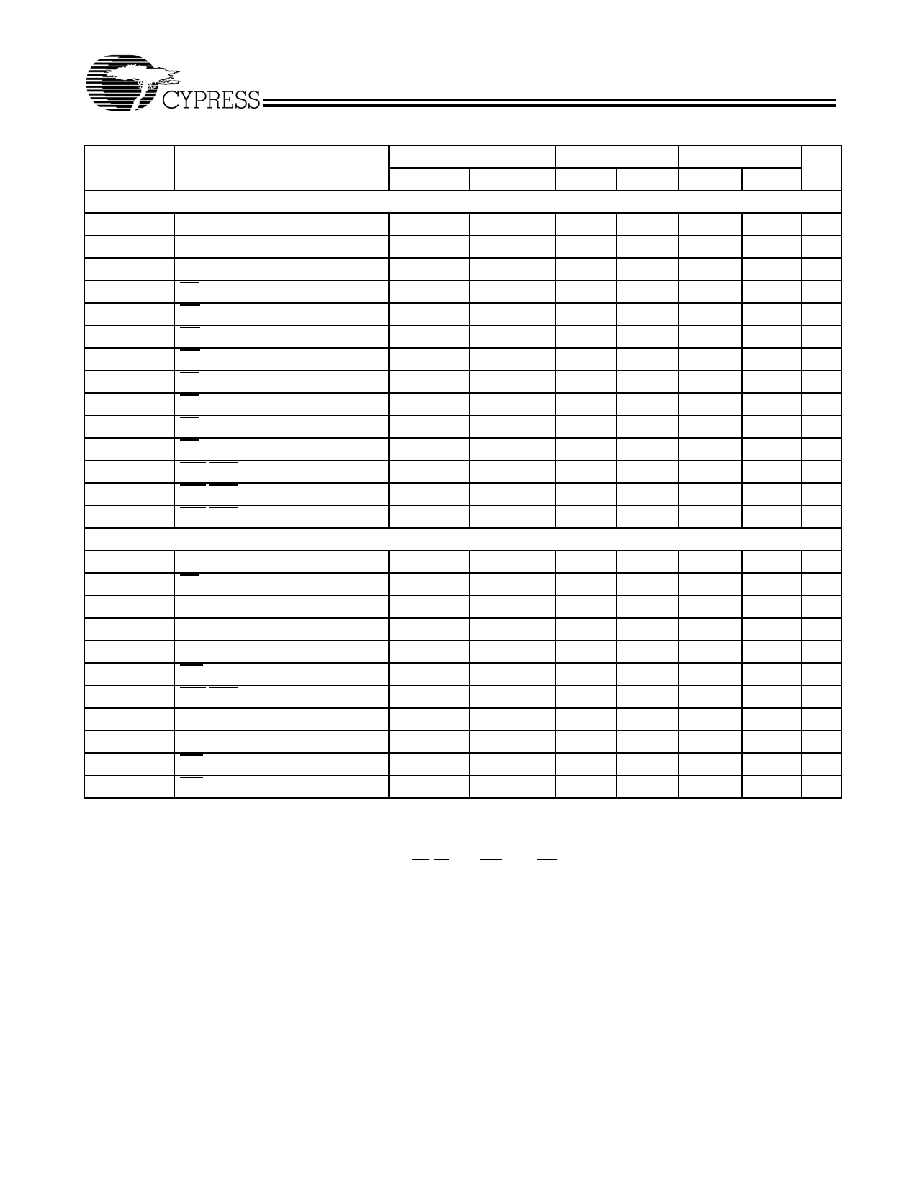
Switching Characteristics (Over the Operating Range)[11]
Parameter
Description
CY62126DV30-45[9]
CY62126DV30-55
CY62126DV30-70
Unit
Min.
Max.
Min.
Max.
Min.
Max.
Read Cycle
tRC
Read Cycle Time
45
55
70
ns
tAA
Address to Data Valid
45
55
70
ns
tOHA
Data Hold from Address Change
10
ns
tACE
CE LOW to Data Valid
45
55
70
ns
tDOE
OE LOW to Data Valid
25
35
ns
tLZOE
OE LOW to Low Z[12]
5
ns
tHZOE
OE HIGH to High Z[12, 13]
15
20
25
ns
tLZCE
CE LOW to Low Z[12]
10
ns
tHZCE
CE HIGH to High Z[12, 13]
20
25
ns
tPU
CE LOW to Power-up
0
ns
tPD
CE HIGH to Power-down
45
55
70
ns
tDBE
BLE/BHE LOW to Data Valid
25
35
ns
tLZBE
BLE/BHE LOW to Low Z[12]
5
ns
tHZBE
BLE/BHE HIGH to High-Z[12, 13]
15
20
25
ns
Write Cycle[14]
tWC
Write Cycle Time
45
55
70
ns
tSCE
CE LOW to Write End
40
60
ns
tAW
Address Set-up to Write End
40
60
ns
tHA
Address Hold from Write End
0
ns
tSA
Address Set-up to Write Start
0
ns
tPWE
WE Pulse Width
35
40
50
ns
tBW
BLE/BHE LOW to Write End
40
60
ns
tSD
Data Set-up to Write End
25
30
ns
tHD
Data Hold from Write End
0
ns
tHZWE
WE LOW to High Z[12, 13]
15
20
25
ns
tLZWE
WE HIGH to Low Z[12]
10
5
ns
Notes:
11. Test conditions assume signal transition time of 1V/ns or less, timing reference levels of VCC(typ.)/2, input pulse levels of 0 to VCC(typ.), and output loading of the
specified IOL.
12. At any given temperature and voltage condition, tHZCE is less than tLZCE, tHZBE is less than tLZBE, tHZOE is less than tLZOE.
13. tHZOE, tHZCE, tHZBE, and tHZWE transitions are measured when the outputs enter a high-impedance state.
14. The internal Write time of the memory is defined by the overlap of WE, CE = VIL, BHE and/or BLE = VIL. All signals must be ACTIVE to initiate a write and any
of these signals can terminate a write by going INACTIVE. The data input set-up and hold timing should be referenced to the edge of the signal that terminates
the write.
相關(guān)PDF資料 |
PDF描述 |
|---|---|
| CY62148L-100SC | 512K X 8 STANDARD SRAM, 100 ns, PDSO32 |
| CY74FCT158ATPC | FCT SERIES, QUAD 2 LINE TO 1 LINE MULTIPLEXER, INVERTED OUTPUT, PDIP16 |
| CY74FCT377ATQC | FCT SERIES, POSITIVE EDGE TRIGGERED D FLIP-FLOP, TRUE OUTPUT, PDSO20 |
| CY7B155-12LC | 16K X 16 STANDARD SRAM, 12 ns, CQCC52 |
| CY7B155-15JC | 16K X 16 STANDARD SRAM, 15 ns, PQCC52 |
相關(guān)代理商/技術(shù)參數(shù) |
參數(shù)描述 |
|---|---|
| CY62126DV30LL-70ZSI | 制造商:CYPRESS 制造商全稱:Cypress Semiconductor 功能描述:1-Mbit (64K x 16) Static RAM |
| CY62126DV30LL-70ZSXI | 制造商:CYPRESS 制造商全稱:Cypress Semiconductor 功能描述:1-Mbit (64K x 16) Static RAM |
| CY62126DV30LL-70ZXI | 制造商:Rochester Electronics LLC 功能描述: 制造商:Cypress Semiconductor 功能描述: |
| CY62126ESL | 制造商:CYPRESS 制造商全稱:Cypress Semiconductor 功能描述:1-Mbit (64K x 16) Static RAM |
| CY62126ESL_13 | 制造商:CYPRESS 制造商全稱:Cypress Semiconductor 功能描述:1-Mbit (64 K x 16) Static RAM |
發(fā)布緊急采購(gòu),3分鐘左右您將得到回復(fù)。