- 您現(xiàn)在的位置:買賣IC網(wǎng) > PDF目錄379056 > CY7C1062DV33 (Cypress Semiconductor Corp.) 16-Mbit (512K X 32) Static RAM PDF資料下載
參數(shù)資料
| 型號: | CY7C1062DV33 |
| 廠商: | Cypress Semiconductor Corp. |
| 英文描述: | 16-Mbit (512K X 32) Static RAM |
| 中文描述: | 16兆位(512k × 32的)靜態(tài)RAM |
| 文件頁數(shù): | 1/10頁 |
| 文件大小: | 310K |
| 代理商: | CY7C1062DV33 |
PRELIMINARY
16-Mbit (512K X 32) Static RAM
CY7C1062DV33
Cypress Semiconductor Corporation
Document #: 38-05477 Rev.*C
198 Champion Court
San Jose
,
CA 95134-1709
408-943-2600
Revised September 4, 2006
Features
High speed
— t
AA
= 10 ns
Low active power
— I
CC
= 150 mA @ 10 ns
Low CMOS standby power
— I
SB2
= 25 mA
Operating voltages of 3.3 ± 0.3V
2.0V data retention
Automatic power-down when deselected
TTL-compatible inputs and outputs
Easy memory expansion with CE
1
, CE
2
, and CE
3
features
Available in Pb-free 119-ball plastic ball grid array
(PBGA) package
Functional Description
The CY7C1062DV33 is a high-performance CMOS Static
RAM organized as 524,288 words by 32 bits.
Writing to the device is accomplished by enabling the chip
(CE
1,
CE
2
and CE
3
LOW) and forcing the Write Enable (WE)
input LOW. If Byte Enable A (B
A
) is LOW, then data from I/O
pins (I/O
0
through I/O
7
), is written into the location specified on
the address pins (A
0
through A
18
). If Byte Enable B (B
B
) is
LOW, then data from I/O pins (I/O
8
through I/O
15
) is written into
the location specified on the address pins (A
0
through A
18
).
Likewise, B
C
and B
D
correspond with the I/O pins I/O
16
to I/O
23
and I/O
24
to I/O
31
, respectively.
Reading from the device is accomplished by enabling the chip
(CE
1,
CE
2
,
and CE
3
LOW) while forcing the Output Enable
(OE) LOW and Write Enable (WE) HIGH. If the first Byte
Enable (B
A
) is LOW, then data from the memory location
specified by the address pins will appear on I/O
0
to I/O
7
. If Byte
Enable B (B
B
) is LOW, then data from memory will appear on
I/O
8
to I/O
15
. Similarly, B
c
and B
D
correspond to the third and
fourth bytes. See the truth table at the back of this data sheet
for a complete description of read and write modes.
The input/output pins (I/O
0
through I/O
31
) are placed in a
high-impedance state when the device is deselected (CE
1,
CE
2
or CE
3
HIGH), the outputs are disabled (OE HIGH), the
byte selects are disabled (B
A-D
HIGH), or during a write
operation (CE
1,
CE
2
, and CE
3
LOW, and WE LOW).
The CY7C1062DV33 is available in 119-ball plastic ball grid
array (PBGA) package.
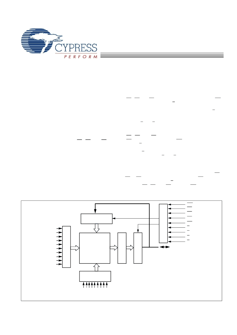
Logic Block Diagram
1
A
1
A
A1
A2
A3
A4
A5
A6
A7
A8
A9
COLUMN
DECODER
R
S
INPUT BUFFERS
512K x 32
ARRAY
A0
A
A
A
A
A
A
A
I/O
0
–I/O
31
OE
B
A
B
B
B
C
CE
3
B
D
O
C
WE
CE
1
CE
2
[+] Feedback
相關(guān)PDF資料 |
PDF描述 |
|---|---|
| CY7C1062DV33-10BGXI | 16-Mbit (512K X 32) Static RAM |
| CY7C1069AV33-10ZXC | 2M x 8 Static RAM |
| CY7C1069AV33-10ZXI | 2M x 8 Static RAM |
| CY7C1069AV33-12ZXC | 2M x 8 Static RAM |
| CY7C1069AV33-12ZXI | 2M x 8 Static RAM |
相關(guān)代理商/技術(shù)參數(shù) |
參數(shù)描述 |
|---|---|
| CY7C1062DV33-10BGI | 功能描述:靜態(tài)隨機(jī)存取存儲器 16-Mbit (512K x 32) 靜態(tài)隨機(jī)存取存儲器 RoHS:否 制造商:Cypress Semiconductor 存儲容量:16 Mbit 組織:1 M x 16 訪問時間:55 ns 電源電壓-最大:3.6 V 電源電壓-最小:2.2 V 最大工作電流:22 uA 最大工作溫度:+ 85 C 最小工作溫度:- 40 C 安裝風(fēng)格:SMD/SMT 封裝 / 箱體:TSOP-48 封裝:Tray |
| CY7C1062DV33-10BGIT | 功能描述:靜態(tài)隨機(jī)存取存儲器 16Mb 512Kx32 靜態(tài)隨機(jī)存取存儲器 RoHS:否 制造商:Cypress Semiconductor 存儲容量:16 Mbit 組織:1 M x 16 訪問時間:55 ns 電源電壓-最大:3.6 V 電源電壓-最小:2.2 V 最大工作電流:22 uA 最大工作溫度:+ 85 C 最小工作溫度:- 40 C 安裝風(fēng)格:SMD/SMT 封裝 / 箱體:TSOP-48 封裝:Tray |
| CY7C1062DV33-10BGXES | 制造商:Cypress Semiconductor 功能描述: |
| CY7C1062DV33-10BGXI | 功能描述:靜態(tài)隨機(jī)存取存儲器 BGA 119 10ns 16Mb RoHS:否 制造商:Cypress Semiconductor 存儲容量:16 Mbit 組織:1 M x 16 訪問時間:55 ns 電源電壓-最大:3.6 V 電源電壓-最小:2.2 V 最大工作電流:22 uA 最大工作溫度:+ 85 C 最小工作溫度:- 40 C 安裝風(fēng)格:SMD/SMT 封裝 / 箱體:TSOP-48 封裝:Tray |
| CY7C1062DV33-10BGXI | 制造商:Cypress Semiconductor 功能描述:IC SRAM 16Mbit 10ns 119-BGA |
發(fā)布緊急采購,3分鐘左右您將得到回復(fù)。