- 您現(xiàn)在的位置:買賣IC網(wǎng) > PDF目錄170347 > CYD18S72AV-133BBI (CYPRESS SEMICONDUCTOR CORP) 256K X 72 DUAL-PORT SRAM, 5.5 ns, PBGA484 PDF資料下載
參數(shù)資料
| 型號(hào): | CYD18S72AV-133BBI |
| 廠商: | CYPRESS SEMICONDUCTOR CORP |
| 元件分類: | SRAM |
| 英文描述: | 256K X 72 DUAL-PORT SRAM, 5.5 ns, PBGA484 |
| 封裝: | 23 X 23 MM, 1.60 MM HEIGHT, 1 MM PITCH, FBGA-484 |
| 文件頁數(shù): | 20/25頁 |
| 文件大小: | 628K |
| 代理商: | CYD18S72AV-133BBI |
CYD04S72V
CYD09S72V
CYD18S72AV
Document #: 38-06069 Rev. *H
Page 4 of 25
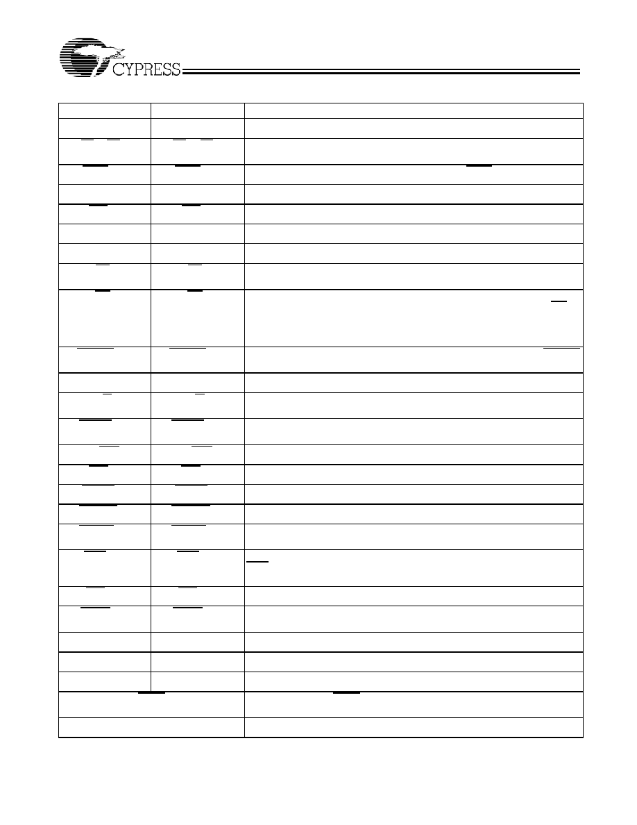
Pin Definitions
Left Port
Right Port
Description
A0L–A17L
A0R–A17R
Address Inputs.
BE0L–BE7L
BE0R–BE7R
Byte Enable Inputs. Asserting these signals enables Read and Write operations
to the corresponding bytes of the memory array.
BUSYL
BUSYR
Port Busy Output. When the collision is detected, a BUSY is asserted.
CL
CR
Input Clock Signal.
CE0L
CE0R
Active Low Chip Enable Input.
CE1L
CE1R
Active High Chip Enable Input.
DQ0L–DQ71L
DQ0R–DQ71R
Data Bus Input/Output.
OEL
OER
Output Enable Input. This asynchronous signal must be asserted LOW to enable
the DQ data pins during Read operations.
INTL
INTR
Mailbox Interrupt Flag Output. The mailbox permits communications between
ports. The upper two memory locations can be used for message passing. INTL is
asserted LOW when the right port writes to the mailbox location of the left port, and
vice versa. An interrupt to a port is deasserted HIGH when it reads the contents of
its mailbox.
LowSPDL
LowSPDR
Port Low Speed Select Input. When operating at less than 100 MHz, the LowSPD
disables the port DLL.
PORTSTD[1:0]L
PORTSTD[1:0]R
Port Address/Control/Data I/O Standard Select Input.
R/WL
R/WR
Read/Write Enable Input. Assert this pin LOW to write to, or HIGH to Read from
the dual-port memory array.
READYL
READYR
Port Ready Output. This signal will be asserted when a port is ready for normal
operation.
CNT/MSKL
CNT/MSKR
Port Counter/Mask Select Input. Counter control input.
ADSL
ADSR
Port Counter Address Load Strobe Input. Counter control input.
CNTENL
CNTENR
[9]
Port Counter Enable Input. Counter control input.
CNTRSTL
CNTRSTR
[8]
Port Counter Reset Input. Counter control input.
CNTINTL
CNTINTR
Port Counter Interrupt Output. This pin is asserted LOW when the unmasked
portion of the counter is incremented to all “1s”.
WRPL
WRPR
[2,3]
Port Counter Wrap Input. After the burst counter reaches the maximum count, if
WRP is low, the unmasked counter bits will be set to 0. If high, the counter will be
loaded with the value stored in the mirror register.
RETL
RETR
Port Counter Retransmit Input. Counter control input.
FTSELL
FTSELR
Flow-Through Select. Use this pin to select Flow-Through mode. When is
de-asserted, the device is in pipelined mode.
VREFL
VREFR
[2,4]
Port External High-Speed IO Reference Input.
VDDIOL
VDDIOR
Port IO Power Supply.
REV[2,4]L
REV[2,4]R
Reserved pins for future features.
MRST
Master Reset Input. MRST is an asynchronous input signal and affects both ports.
A master reset operation is required at power-up.
TRST[2,5]
JTAG Reset Input.
相關(guān)PDF資料 |
PDF描述 |
|---|---|
| CYDD18S72V18-167BGI | 256K X 72 DUAL-PORT SRAM, 9 ns, PBGA484 |
| CYW2330ZITR | PLL FREQUENCY SYNTHESIZER, 2500 MHz, PDSO20 |
| CYW311OXCT | 200 MHz, PROC SPECIFIC CLOCK GENERATOR, PDSO48 |
| CZ23EH-FREQ-OUT23 | VCXO, CLOCK, 1.25 MHz - 65 MHz, CMOS/TTL OUTPUT |
| CZM4-2000 | VCO, 1950 MHz - 2800 MHz |
相關(guān)代理商/技術(shù)參數(shù) |
參數(shù)描述 |
|---|---|
| CYD18S72V | 制造商:CYPRESS 制造商全稱:Cypress Semiconductor 功能描述:FLEx72⑩ 3.3V 64K/128K/256K x 72 Synchronous Dual-Port RAM |
| CYD18S72V-100BBC | 功能描述:靜態(tài)隨機(jī)存取存儲(chǔ)器 18M (256Kx72) 3.3v 100MHz Synch 靜態(tài)隨機(jī)存取存儲(chǔ)器 RoHS:否 制造商:Cypress Semiconductor 存儲(chǔ)容量:16 Mbit 組織:1 M x 16 訪問時(shí)間:55 ns 電源電壓-最大:3.6 V 電源電壓-最小:2.2 V 最大工作電流:22 uA 最大工作溫度:+ 85 C 最小工作溫度:- 40 C 安裝風(fēng)格:SMD/SMT 封裝 / 箱體:TSOP-48 封裝:Tray |
| CYD18S72V-100BBI | 功能描述:靜態(tài)隨機(jī)存取存儲(chǔ)器 18M (256Kx72) 3.3v 100MHz Synch 靜態(tài)隨機(jī)存取存儲(chǔ)器 RoHS:否 制造商:Cypress Semiconductor 存儲(chǔ)容量:16 Mbit 組織:1 M x 16 訪問時(shí)間:55 ns 電源電壓-最大:3.6 V 電源電壓-最小:2.2 V 最大工作電流:22 uA 最大工作溫度:+ 85 C 最小工作溫度:- 40 C 安裝風(fēng)格:SMD/SMT 封裝 / 箱體:TSOP-48 封裝:Tray |
| CYD18S72V-100BBXC | 制造商:CYPRESS 制造商全稱:Cypress Semiconductor 功能描述:FLEx72⑩ 3.3V 64K/128K/256K x 72 Synchronous Dual-Port RAM |
| CYD18S72V-100BBXI | 制造商:CYPRESS 制造商全稱:Cypress Semiconductor 功能描述:FLEx72⑩ 3.3V 64K/128K/256K x 72 Synchronous Dual-Port RAM |
發(fā)布緊急采購,3分鐘左右您將得到回復(fù)。