- 您現(xiàn)在的位置:買賣IC網(wǎng) > PDF目錄10362 > D2-45057-QR-T (Intersil)IC DGTL AMP PWM CTRLR 68QFN PDF資料下載
參數(shù)資料
| 型號(hào): | D2-45057-QR-T |
| 廠商: | Intersil |
| 文件頁(yè)數(shù): | 14/31頁(yè) |
| 文件大?。?/td> | 0K |
| 描述: | IC DGTL AMP PWM CTRLR 68QFN |
| 標(biāo)準(zhǔn)包裝: | 3,000 |
| 系列: | D2Audio™ |
| 類型: | D 類 |
| 輸出類型: | 2 通道(立體聲) |
| 在某負(fù)載時(shí)最大輸出功率 x 通道數(shù)量: | 30W x 1 @ 8 歐姆 |
| 電源電壓: | 9 V ~ 26 V |
| 安裝類型: | 表面貼裝 |
| 供應(yīng)商設(shè)備封裝: | 68-QFN 裸露焊盤(10x10) |
| 封裝/外殼: | 68-VFQFN 裸露焊盤 |
| 包裝: | 帶卷 (TR) |
第1頁(yè)第2頁(yè)第3頁(yè)第4頁(yè)第5頁(yè)第6頁(yè)第7頁(yè)第8頁(yè)第9頁(yè)第10頁(yè)第11頁(yè)第12頁(yè)第13頁(yè)當(dāng)前第14頁(yè)第15頁(yè)第16頁(yè)第17頁(yè)第18頁(yè)第19頁(yè)第20頁(yè)第21頁(yè)第22頁(yè)第23頁(yè)第24頁(yè)第25頁(yè)第26頁(yè)第27頁(yè)第28頁(yè)第29頁(yè)第30頁(yè)第31頁(yè)
D2-45057, D2-45157
21
FN6785.0
July 29, 2010
mode that is defined by these pins’ logic state. These
device pins are strapped either high or low on the
system’s design (PCB), and it is the state of these pins
that is latched into, and defines boot mode operation.
Boot Modes
The D2-45057, D2-45157 devices contain embedded
firmware to operate the part and run the amplifier
system. Parameter information that is used by the
programmable settings can be written to the device after
it is operational and running. However, parameter data
can also be read at boot time, allowing saved parameter
settings to be used, or allowing amplifier function to be
set through a system microcontroller interface. The
device is designed to boot in one of four possible boot
modes, allowing control and data to be provided through
these boot sources:
I2C Slave (to external Microcontroller)
I2C EEPROM
Internal Device ROM Only
SPI Slave
The specific boot mode is selected based on the state of
the IRQB and IRQA input pins at the time of reset
de-assertion. Boot modes and their functions are shown
in Table 4. (Note: “Boot Mode” describes the “mode” of
device initialization with respect to the source of
parameter data or start-up control settings. This is not to
be confused with “Output Mode” or audio processing
“Configuration Mode” settings that define
amplifier-specific functions.)
The device initializes as defined by its boot mode. But it
gets its configuration and parameter data from the host
device. This host device can be either an external
controller, or from an EEPROM. If a system uses both an
external controller and an EEPROM, the EEPROM will load
first, and during this time, the controller must remain off
the I2C bus until after the reading sequence from
EEPROM has completed.
Power Supply Requirements
The device requires operating power for these voltages:
PWMVDD and RVDD:
- 3.3V DC Supply Voltage.
- RVDD operates interface and I/O logic.
- PWMVDD is the same voltage, and is used for the
PWM outputs and output stage drive.
CVDD and PLLVDD
- 1.8V DC Supply Voltage
- CVDD operates the internal processor and DSP core.
- PLLVDD also operates at the internal processor
voltage levels, but is provided through a separate
connection to allow isolation and bypassing for
noise and performance improvements.
“High Voltage” (HVDD[A:D], and VDDHV)
- HVDDA, HVDDB, HVDDC, and HVDDD are the
“High Voltage” supplies used for operating each of
the four output power stages.
- VDDHV is used as the source for the on-chip +5V
regulator that is used for the output stage drivers.
- Individual power (HVDD[A:D]) and their
corresponding ground (HGND[A:D]) pins are
included for each of the four power stage outputs,
providing channel isolation and low impedance
source connections to each of the outputs. All the
HVDD[A:D]/VDDHV pins connect to the same
voltage source.
High-Side Gate Drive Voltage
An on-chip bootstrap circuit provides the gate drive
voltage used by each output stage. A pin is included for
each output channel (HSBS[A:D]) for connection of a
capacitor (nominal, 0.22F/50V) from this pin to that
channel’s PWM output.
Drivers for high-side FETs on the output stages require a
voltage above the supply used for powering that FET. The
charge pumping action of the driving PWM to this driver
produces this “bootstrap” voltage, and uses this capacitor
to filter and hold this gate drive voltage. This enables
amplifier operation without need of connection to an
additional power supply voltage.
Power Supply Synchronization
The the PSSYNC/CFG1 pin provides a power supply
synchronization signal for switching power supplies.
Firmware configures this pin to the frequency and duty
cycle needed by the system switching regulator. This
synchronization allows switching supplies used with the
device to operate without generating in-band audio
interference signals that could be possible if the switching
power supply is not locked to the amplifier switching.
This PSSYNC/CFG1 pin is a shared pin. (Refer to multiple-
device reset and initialization, it operates as one of two
configuration input pins, where its high or low logic state
is used to set the amplifier configuration mode. After
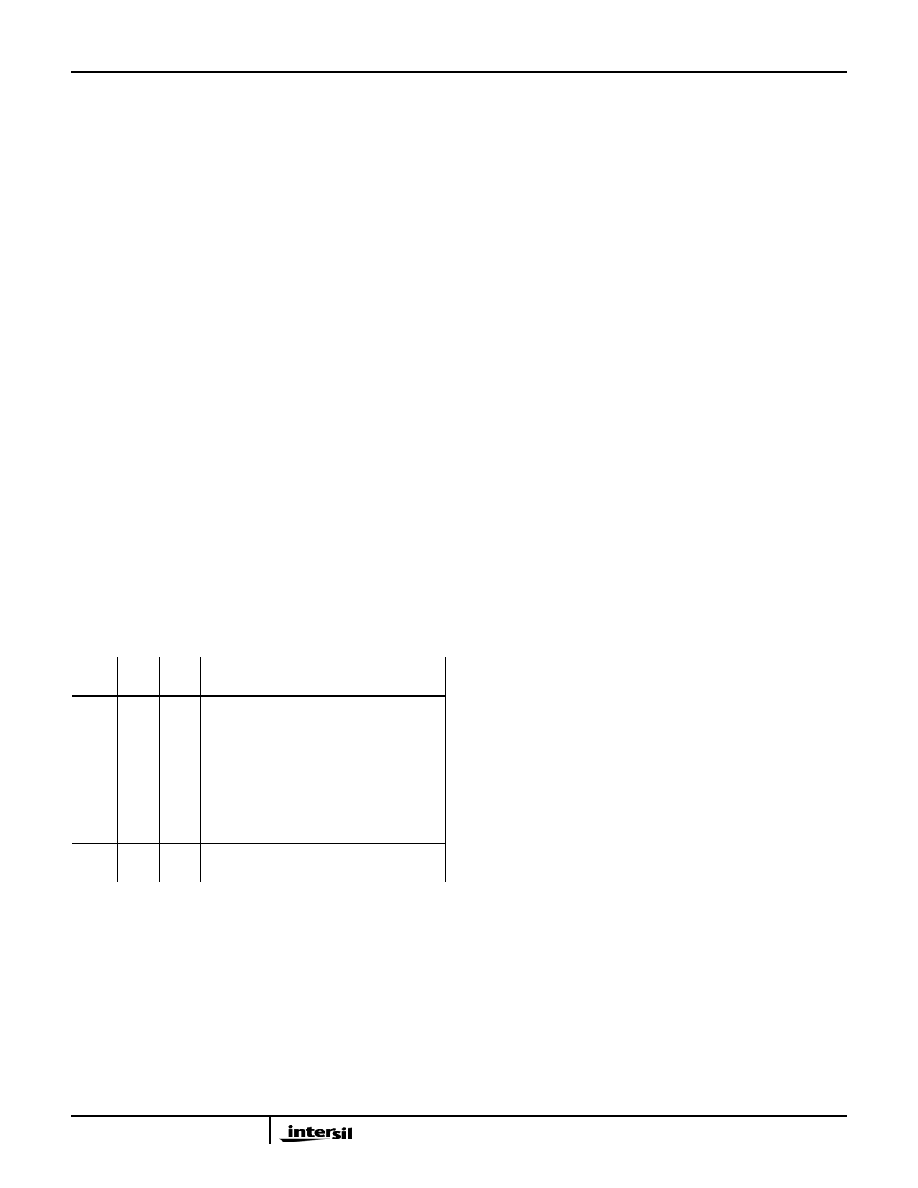
TABLE 4. BOOT MODE SETTINGS
BOOT
MODE
IRQB
PIN
IRQA
PIN
MASTER/
SLAVE
DESCRIPTION
00
0
I2C Slave Operates as I2C slave, boot
at address 0x88. An external
2-wire I2C master provides
the boot code.
10
1
I2C Master Operates as 2-wire master;
loads boot code from ROM on
I2C port.
2
1
0
-
Internal ROM Boot/Operation
3
1
SPI Slave SPI slave. External SPI
master provides boot code.
相關(guān)PDF資料 |
PDF描述 |
|---|---|
| D38999/26WD5BN | CONN HSG PLUG 5POS STRGHT SCKT |
| D38999/24WD97SNLC | CONN HSG RCPT 12POS JAM NUT SCKT |
| VI-B6P-IV-F2 | CONVERTER MOD DC/DC 13.8V 150W |
| VI-B6N-IV-F3 | CONVERTER MOD DC/DC 18.5V 150W |
| D38999/20MC98BN | CONN HSG RCPT 10POS WALL MT SCKT |
相關(guān)代理商/技術(shù)參數(shù) |
參數(shù)描述 |
|---|---|
| D2450B | 制造商:未知廠家 制造商全稱:未知廠家 功能描述: |
| D2450-B | 功能描述:固態(tài)繼電器-工業(yè)安裝 PM IP00 280VAC/50A , 3-32VDC In, ZC RoHS:否 制造商:Crydom 控制電壓范圍:4 VDC to 32 VDC 負(fù)載電壓額定值:7 VDC to 72 VDC 負(fù)載電流額定值:160 A 觸點(diǎn)形式: 輸出設(shè)備:SSR 安裝風(fēng)格:Panel |
| D2450B10 | 制造商:未知廠家 制造商全稱:未知廠家 功能描述: |
| D2450-C3 | 制造商:C3 semi 功能描述: |
| D2450E | 制造商:未知廠家 制造商全稱:未知廠家 功能描述: |
發(fā)布緊急采購(gòu),3分鐘左右您將得到回復(fù)。