- 您現(xiàn)在的位置:買賣IC網(wǎng) > PDF目錄376558 > DAC667 (Texas Instruments, Inc.) Microprocessor-Compatible 12-Bit Dightal-To-Analog Converter(與微處理器兼容的12位D/A轉(zhuǎn)換器) PDF資料下載
參數(shù)資料
| 型號(hào): | DAC667 |
| 廠商: | Texas Instruments, Inc. |
| 英文描述: | Microprocessor-Compatible 12-Bit Dightal-To-Analog Converter(與微處理器兼容的12位D/A轉(zhuǎn)換器) |
| 中文描述: | 微處理器兼容的12位Dightal到模擬轉(zhuǎn)換器(與微處理器兼容的12位的D / A轉(zhuǎn)換器) |
| 文件頁數(shù): | 3/9頁 |
| 文件大?。?/td> | 218K |
| 代理商: | DAC667 |
3
DAC667
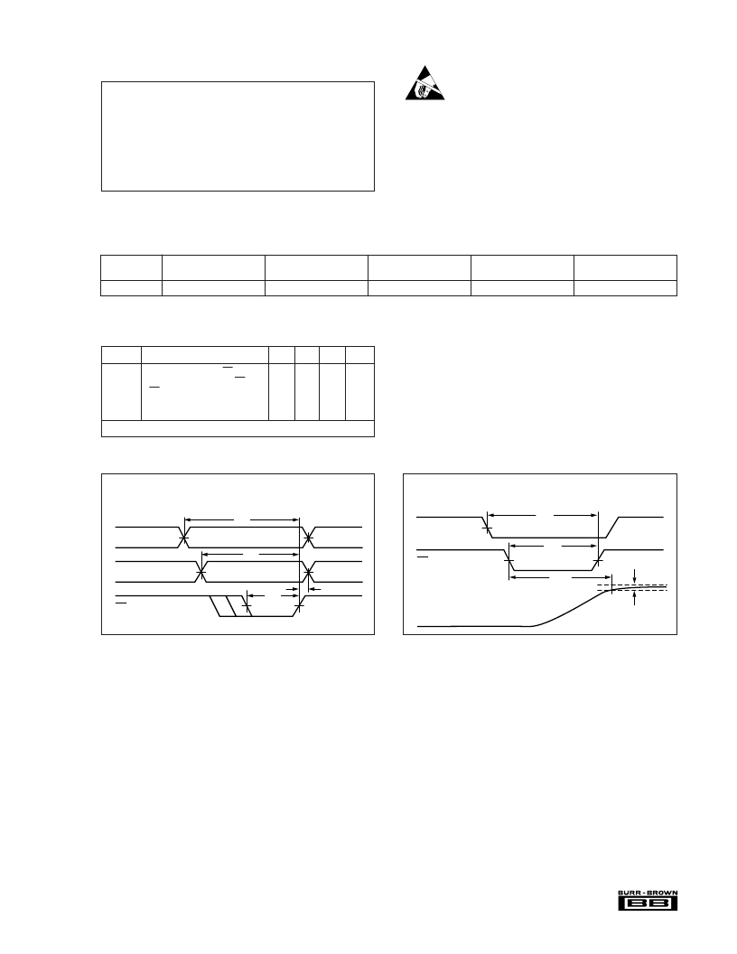
TIMING SPECIFICATIONS
SYMBOL
PARAMETER
MIN
TYP
MAX
UNITS
t
DC
t
AC
t
CP
t
DH
t
SETT
Data Valid to End of CS
Address Valid to End of CS
CS Pulse Width
Data Hold Time
Output Voltage Settling Time
50
100
100
0
–
–
–
–
–
2
–
–
–
–
4
ns
ns
ns
ns
μ
s
All models, T
A
= +25
°
C, V
CC
= +12V or +15V, V
EE
= –12V or –15V.
ABSOLUTE MAXIMUM RATINGS
V
CC
to Power Ground ..............................................................0V to +18V
V
to Power Ground ..............................................................0V to –18V
Digital Inputs (Pins 11–15, 17–28) to Power Ground.............–1V to +7V
Ref In to Reference Ground..............................................................
±
12V
Bipolar Offset to Reference Ground .................................................
±
12V
10V Span Resistor to Reference Ground .........................................
±
12V
20V Span Resistor to Reference Ground .........................................
±
24V
Ref Out, V
OUT
(Pins 6, 9) ....................Indefinite Short to Power Ground,
Momentary Short To V
CC
Power Dissipation ........................................................................1000mW
ELECTROSTATIC
DISCHARGE SENSITIVITY
This integrated circuit can be damaged by ESD. Burr-Brown
recommends that all integrated circuits be handled with
appropriate precautions. Failure to observe proper handling
and installation procedures can cause damage.
ESD damage can range from subtle performance degradation
to complete device failure. Precision integrated circuits may
be more susceptible to damage because very small parametric
changes could cause the device not to meet its published
specifications.
PACKAGE/ORDERING INFORMATION
TEMPERATURE
RANGE
LINEARITY ERROR
max at 25
°
C
±
1/2LSB
GAIN TC, max
(ppm/
°
C)
±
30
PACKAGE DRAWING
NUMBER
(1)
PRODUCT
PACKAGE
DAC667JP
28-Pin Plastic DIP
0
°
C to +70
°
C
215
NOTE: (1) For detailed drawing and dimension table, please see end of data sheet, or Appendix C of Burr-Brown IC Data Book.
TIMING DIAGRAMS
Load first rank from Data Bus; A3 = 1.
t
Write Cycle #1
t
SETT
CS
±1/2LSB
A3
t
AC
t
CP
Load second rank from first rank; A2, A1, A0 = 1.
Write Cycle #2
Output
CS
A2–A0
t
AC
t
DC
t
DH
t
CP
DB11–DB0
相關(guān)PDF資料 |
PDF描述 |
|---|---|
| DAC667 | |
| DAC667JP | IC-12-BIT DAC |
| DAC701 | Monolithic 16-Bit DIGITAL-TO-ANALOG CONVERTERS |
| DAC702 | Monolithic 16-Bit DIGITAL-TO-ANALOG CONVERTERS |
| DAC703B | Monolithic 16-Bit DIGITAL-TO-ANALOG CONVERTERS |
相關(guān)代理商/技術(shù)參數(shù) |
參數(shù)描述 |
|---|---|
| DAC667AH | 制造商:BURR-BROWN 功能描述: |
| DAC667BH | 制造商:BB 功能描述:_ |
| DAC667JP | 制造商:Rochester Electronics LLC 功能描述:- Bulk 制造商:Texas Instruments 功能描述: |
| DAC667KP | 制造商:Rochester Electronics LLC 功能描述:- Bulk 制造商:BURR-BROWN 功能描述: 制造商:Texas Instruments 功能描述: |
| DAC-6-CG | 制造商:Thomas & Betts 功能描述:2" RIGID TF CONDUIT BODY 制造商:Thomas & Betts 功能描述:Universal Recessed Box And Cover |
發(fā)布緊急采購,3分鐘左右您將得到回復(fù)。