- 您現(xiàn)在的位置:買賣IC網(wǎng) > PDF目錄376597 > DDC118IRTCT Octal Current Input 20-Bit Analog-To-Digital Converter PDF資料下載
參數(shù)資料
| 型號: | DDC118IRTCT |
| 英文描述: | Octal Current Input 20-Bit Analog-To-Digital Converter |
| 中文描述: | 八路電流輸入20位模擬數(shù)字轉(zhuǎn)換器 |
| 文件頁數(shù): | 9/30頁 |
| 文件大小: | 384K |
| 代理商: | DDC118IRTCT |
第1頁第2頁第3頁第4頁第5頁第6頁第7頁第8頁當(dāng)前第9頁第10頁第11頁第12頁第13頁第14頁第15頁第16頁第17頁第18頁第19頁第20頁第21頁第22頁第23頁第24頁第25頁第26頁第27頁第28頁第29頁第30頁
""#
SBAS325A JUNE 2004 REVISED JUNE 2005
www.ti.com
9
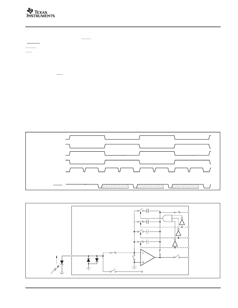
The digital interface of the DDC118 provides the digital
results via a synchronous serial interface consisting of
differential data clocks (DCLK and DCLK), a valid data pin
(DVALID), differential serial data output pins (DOUT and
DOUT), and differential serial data input pins (DIN and
DIN). The DDC118 contains only four A/D converters, so
the conversion process is interleaved (see Figure 2). The
integration and conversion process is fundamentally
independent of the data retrieval process. Consequently,
the CLK frequency and DCLK frequencies need not be the
same. DIN and DIN are only used when multiple
converters are cascaded and should be tied to DGND and
DVDD otherwise.
DEVICE OPERATION
Basic Integration Cycle
The topology of the front end of the DDC118 is an analog
integrator as shown in Figure 3. In this diagram, only Input
IN1 is shown. This representation of the input stage
consists of an operational amplifier, a selectable feedback
capacitor network (C
F
), and several switches that
implement the integration cycle. The timing relationships
of all of the switches shown in Figure 3 are illustrated in
Figure 4. Figure 4 is used to conceptualize the operation
of the integrator input stage of the DDC118 and should not
be used as an exact timing tool for design. See Figure 5 for
the block diagrams of the reset, integrate, wait and convert
states of the integrator section of the DDC118. This
internal switching network is controlled externally with the
convert
pin
(CONV),
(RANGE0-RANGE2), and the system clock (CLK). For the
best noise performance, CONV must be synchronized
with the rising edge of CLK. It is recommended that CONV
toggle within
±
10ns of the rising edge of CLK.
range
selection
pins
The noninverting inputs of the integrators are connected to
ground. Consequently, the DDC118 analog ground should
be as clean as possible. The range switches, along with
the internal and external capacitors (C
F
), are shown in
parallel between the inverting input and output of the
operational amplifier. At the beginning of a conversion, the
switches S
A/D
, S
INTA
, S
INTB
, S
REF1
, S
REF2
, and S
RESET
are set (see Figure 4).
IN1, IN2, IN5, and IN6,
Integrator A
IN1, IN2, IN5, and IN6,
Integrator B
IN3, IN4, IN7, and IN8,
Integrator A
IN3, IN4, IN7, and IN8,
Integrator B
Conversion in Progress
DVALID
IN1B
IN2B
IN5B
IN6B
IN3B
IN4B
IN7B
IN8B
IN1A
IN2A
IN5A
IN6A
Integrate
Integrate
Integrate
Integrate
Integrate
Integrate
Integrate
Integrate
IN3A
IN4A
IN7A
IN8A
IN1B
IN2B
IN5B
IN6B
IN3B
IN4B
IN7B
IN8B
IN1A
IN2A
IN5A
IN6A
IN3A
IN4A
IN7A
IN8A
Figure 2. Basic Integration and Conversion Timing for the DDC118 (continuous mode)
50pF
25pF
12.5pF
VREF
RANGE2
RANGE1
RANGE0
To Converter
S
RESET
S
REF2
S
A/D1A
S
INTA
S
REF1
S
INTB
IN1
ESD
Protection
Diodes
Input
Current
Integrator A
Integrator B (same as A)
Photodiode
3pF
Figure 3. Basic Integration Configuration for Input 1, shown with a 250pC (C
F
= 62.5pF) Input Range
相關(guān)PDF資料 |
PDF描述 |
|---|---|
| DDG-GJS-K1 | LED GaP |
| DDR-GJS-J2L1-1-I1 | LED GaP |
| DDR-GJS-K1 | LED GaP |
| DDR-GJS-K2 | LED GaP |
| DDR-GJS-L1 | LED GaP |
相關(guān)代理商/技術(shù)參數(shù) |
參數(shù)描述 |
|---|---|
| DDC118IRTCT | 制造商:Texas Instruments 功能描述:IC ADC 20BIT OCTAL 48-VQFN |
| DDC118IRTCT | 制造商:Texas Instruments 功能描述:A/D CONVERTER (A-D) IC ((NW)) |
| DDC118IRTCTG4 | 功能描述:模數(shù)轉(zhuǎn)換器 - ADC Octal Current-Input 20-Bit RoHS:否 制造商:Texas Instruments 通道數(shù)量:2 結(jié)構(gòu):Sigma-Delta 轉(zhuǎn)換速率:125 SPs to 8 KSPs 分辨率:24 bit 輸入類型:Differential 信噪比:107 dB 接口類型:SPI 工作電源電壓:1.7 V to 3.6 V, 2.7 V to 5.25 V 最大工作溫度:+ 85 C 安裝風(fēng)格:SMD/SMT 封裝 / 箱體:VQFN-32 |
| DDC11XEVM-PDK | 功能描述:數(shù)據(jù)轉(zhuǎn)換 IC 開發(fā)工具 DDC11xEVM-PDK Eval Mod RoHS:否 制造商:Texas Instruments 產(chǎn)品:Demonstration Kits 類型:ADC 工具用于評估:ADS130E08 接口類型:SPI 工作電源電壓:- 6 V to + 6 V |
| DDC122LH | 制造商:DIODES 制造商全稱:Diodes Incorporated 功能描述:NPN PRE-BIASED SMALL SIGNAL SOT-563 DUAL SURFACE MOUNT TRANSISTOR |
發(fā)布緊急采購,3分鐘左右您將得到回復(fù)。