- 您現(xiàn)在的位置:買賣IC網(wǎng) > PDF目錄1915 > DS3164+ (Maxim Integrated Products)IC ATM/PACKET PHY QUAD 400-BGA PDF資料下載
參數(shù)資料
| 型號(hào): | DS3164+ |
| 廠商: | Maxim Integrated Products |
| 文件頁數(shù): | 112/384頁 |
| 文件大?。?/td> | 0K |
| 描述: | IC ATM/PACKET PHY QUAD 400-BGA |
| 產(chǎn)品培訓(xùn)模塊: | Lead (SnPb) Finish for COTS Obsolescence Mitigation Program |
| 標(biāo)準(zhǔn)包裝: | 1 |
| 類型: | PHY 收發(fā)器 |
| 應(yīng)用: | 測試設(shè)備 |
| 安裝類型: | 表面貼裝 |
| 封裝/外殼: | 400-BBGA |
| 供應(yīng)商設(shè)備封裝: | 400-PBGA(27x27) |
| 包裝: | 托盤 |
第1頁第2頁第3頁第4頁第5頁第6頁第7頁第8頁第9頁第10頁第11頁第12頁第13頁第14頁第15頁第16頁第17頁第18頁第19頁第20頁第21頁第22頁第23頁第24頁第25頁第26頁第27頁第28頁第29頁第30頁第31頁第32頁第33頁第34頁第35頁第36頁第37頁第38頁第39頁第40頁第41頁第42頁第43頁第44頁第45頁第46頁第47頁第48頁第49頁第50頁第51頁第52頁第53頁第54頁第55頁第56頁第57頁第58頁第59頁第60頁第61頁第62頁第63頁第64頁第65頁第66頁第67頁第68頁第69頁第70頁第71頁第72頁第73頁第74頁第75頁第76頁第77頁第78頁第79頁第80頁第81頁第82頁第83頁第84頁第85頁第86頁第87頁第88頁第89頁第90頁第91頁第92頁第93頁第94頁第95頁第96頁第97頁第98頁第99頁第100頁第101頁第102頁第103頁第104頁第105頁第106頁第107頁第108頁第109頁第110頁第111頁當(dāng)前第112頁第113頁第114頁第115頁第116頁第117頁第118頁第119頁第120頁第121頁第122頁第123頁第124頁第125頁第126頁第127頁第128頁第129頁第130頁第131頁第132頁第133頁第134頁第135頁第136頁第137頁第138頁第139頁第140頁第141頁第142頁第143頁第144頁第145頁第146頁第147頁第148頁第149頁第150頁第151頁第152頁第153頁第154頁第155頁第156頁第157頁第158頁第159頁第160頁第161頁第162頁第163頁第164頁第165頁第166頁第167頁第168頁第169頁第170頁第171頁第172頁第173頁第174頁第175頁第176頁第177頁第178頁第179頁第180頁第181頁第182頁第183頁第184頁第185頁第186頁第187頁第188頁第189頁第190頁第191頁第192頁第193頁第194頁第195頁第196頁第197頁第198頁第199頁第200頁第201頁第202頁第203頁第204頁第205頁第206頁第207頁第208頁第209頁第210頁第211頁第212頁第213頁第214頁第215頁第216頁第217頁第218頁第219頁第220頁第221頁第222頁第223頁第224頁第225頁第226頁第227頁第228頁第229頁第230頁第231頁第232頁第233頁第234頁第235頁第236頁第237頁第238頁第239頁第240頁第241頁第242頁第243頁第244頁第245頁第246頁第247頁第248頁第249頁第250頁第251頁第252頁第253頁第254頁第255頁第256頁第257頁第258頁第259頁第260頁第261頁第262頁第263頁第264頁第265頁第266頁第267頁第268頁第269頁第270頁第271頁第272頁第273頁第274頁第275頁第276頁第277頁第278頁第279頁第280頁第281頁第282頁第283頁第284頁第285頁第286頁第287頁第288頁第289頁第290頁第291頁第292頁第293頁第294頁第295頁第296頁第297頁第298頁第299頁第300頁第301頁第302頁第303頁第304頁第305頁第306頁第307頁第308頁第309頁第310頁第311頁第312頁第313頁第314頁第315頁第316頁第317頁第318頁第319頁第320頁第321頁第322頁第323頁第324頁第325頁第326頁第327頁第328頁第329頁第330頁第331頁第332頁第333頁第334頁第335頁第336頁第337頁第338頁第339頁第340頁第341頁第342頁第343頁第344頁第345頁第346頁第347頁第348頁第349頁第350頁第351頁第352頁第353頁第354頁第355頁第356頁第357頁第358頁第359頁第360頁第361頁第362頁第363頁第364頁第365頁第366頁第367頁第368頁第369頁第370頁第371頁第372頁第373頁第374頁第375頁第376頁第377頁第378頁第379頁第380頁第381頁第382頁第383頁第384頁
DS3161/DS3162/DS3163/DS3164
2
FEATURES (continued)
Full-Featured DS3/E3/PLCP Alarm Generation
and Detection
Built-In HDLC Controllers with 256-Byte FIFOs
for Insertion/Extraction of DS3 PMDL, G.751 Sn
Bit, and G.832 NR/GC Bytes and PLCP NR/GC
Bytes
On-Chip BERTs for PRBS and Repetitive Pattern
Generation, Detection, and Analysis
Large Performance-Monitoring Counters for
Accumulation Intervals of at Least 1 Second
Flexible Overhead Insertion/Extraction Ports for
DS3, E3, and PLCP Framers
Pin and Software Compatible with DS3181–
DS3184 Single–Quad ATM/Packet PHYs with
Built-In LIUs and DS3171–DS3174 Single–Quad
DS3/E3 Single-Chip Transceivers—Framers and
LIUs
DETAILED DESCRIPTION
The DS3161 (single), DS3162 (dual), DS3163 (triple), and DS3164 (quad) PHYs perform all the functions
necessary for mapping/demapping ATM cells and/or packets into as many as four DS3 (44.736Mbps) framed, E3
(34.368Mbps) framed, or 52Mbps clear-channel data streams. Dedicated cell processor and packet processor
blocks prepare outgoing cells or packets for transmission and check incoming cells or packets upon arrival. Built-in
DS3/E3 framers transmit and receive cell/packet data in properly formatted M23 DS3, C-bit DS3, G.751 E3, or
G.832 E3 data streams. PLCP framers provide legacy ATM transmission-convergence support. DSS scrambling is
performed for clear-channel ATM cell support. With integrated hardware support for both cells and packets, the
DS316x DS3/E3 ATM/Packet PHYs provide system-on-chip solutions (from DS3/E3/STS-1 digital lines to
ATM/Packet UTOPIA/POS-PHY Level 2/3 system switch) for universal high-density line cards in the unchannelized
DS3/E3/clear-channel DS3 ATM/Packet applications. Unused functions can be powered down to reduce device
power. The DS316x ATM/Packet PHYs with embedded framers conform to the telecommunications standards
listed in Section 4.
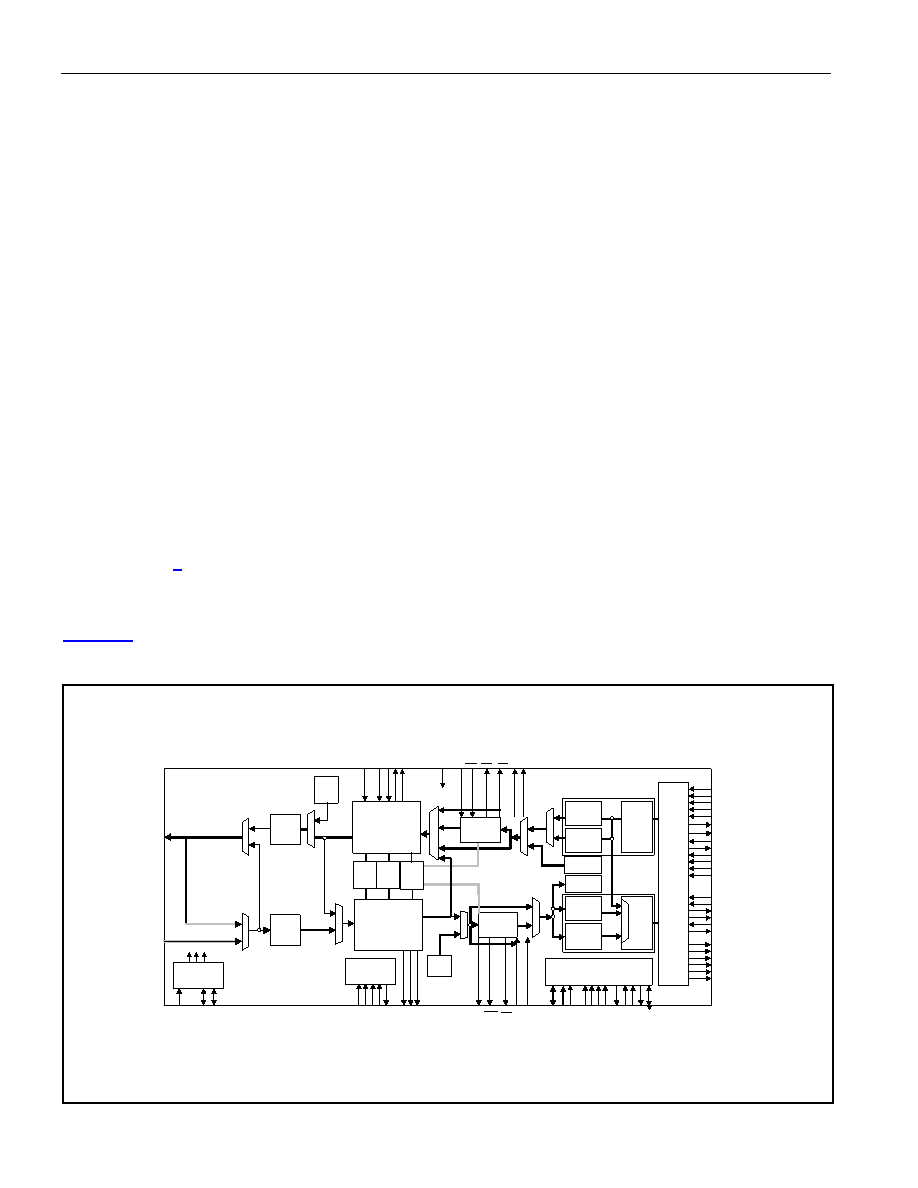
1 BLOCK DIAGRAM
Figure 1-1 shows the functional block diagram of one channel ATM/Packet PHY.
Figure 1-1. DS316x Functional Block Diagram
IEEE P1149.1
JTAG Test
Access Port
Microprocessor
Interface
HDLC
FEAC
LLB
DLB
DS3 / E3
Transmit
Formatter
DS3 / E3
Receive
Framer
Trail
Trace
Buffer
Tx Cell
Processor
Tx
FIFO
S
yst
em
In
te
rf
ac
e
Rx
Cell
Processor
Rx
FIFO
Tx Packet
Processor
SL
B
Rx
Packet
Processor
TAIS
TUA1
TX
FRAC/
PLCP
RX FRAC/
PLCP
Clock
Rate
Adapter
TX BERT
RX BERT
PL
B
ALB
UA1
GEN
B3ZS/
HDB3
Encoder
B3ZS/
HDB3
Decoder
TSCLK
TADR[4:0]
TDATA[31:0]
TPRTY
TEN
TDXA[4:2]
TSOX
TEOP
TSPA
TSX
TMOD[1:0]
TERR
RSCLK
RADR[4:0]
RDATA[31:0]
RPRTY
REN
RDXA[4:2]
RSOX
REOP
RVAL
RMOD[1:0]
RERR
TDXA[1]/TPXA
/RSX
n = port #
D[
15:
0]
A[
10:
1]
ALE CS
RD
/DS
WR
/R/
W
JTDO
JTCLK JTM
S
JTDI
JTRST
ROHn
ROHCLKn ROHSOFn
RPOHn/
RSERn
RPOHCLKn/
RCLKOn/
RPOHSOFn/
R
SOFOn/
RDENn/
RFOHENOn
CLKA
CLKB
CLKC
RFOHENIn/
MODE
INT
GP
IO[8
:1
]
WIDT
H
RDY
RPDENIn
RPDATn
RGCLKn
A[
0]
/BSWAP
TPOHSOFn/
TSOFOn/
TDENn\
TFOHENOn
TOHn TOHCLKn TOHSOFn
TCLKI
n
TOHENn
TPOHCLKN/
TCLKOn/
T
GCLKn
TOHMI
n/
T
SOFI
n
TPOHn/
TFOHn/
T
SERn
TPOHENn/
TFOHENI
n/
TPDENIn
TPDENOn
TPDATn
RLCLKn
TPOSn/
TDATn
TNEGn/
TOHMOn/
TLCLKn
RDATn
RPOSn/
RNEGn/
RLCVn/
ROHMIn
DS316x
相關(guān)PDF資料 |
PDF描述 |
|---|---|
| DS3170+ | IC TXRX DS3/E3 100-CSBGA |
| DS3172N+ | IC TXRX DS3/E3 DUAL 400-BGA |
| DS3181N+ | IC ATM/PACKET PHY W/LIU 400PBGA |
| DS32512N+ | IC LIU DS3/E3/STS-1 12P 484-BGA |
| DS3254N+ | IC LIU DS3/E3/STS-1 144-CSBGA |
相關(guān)代理商/技術(shù)參數(shù) |
參數(shù)描述 |
|---|---|
| DS3164+ | 功能描述:網(wǎng)絡(luò)控制器與處理器 IC Quad ATM/Packet PHYs for DS3/E3/STS-1 RoHS:否 制造商:Micrel 產(chǎn)品:Controller Area Network (CAN) 收發(fā)器數(shù)量: 數(shù)據(jù)速率: 電源電流(最大值):595 mA 最大工作溫度:+ 85 C 安裝風(fēng)格:SMD/SMT 封裝 / 箱體:PBGA-400 封裝:Tray |
| DS316-409NR WAF | 制造商:ON Semiconductor 功能描述: |
| DS3164DK | 功能描述:網(wǎng)絡(luò)開發(fā)工具 RoHS:否 制造商:Rabbit Semiconductor 產(chǎn)品:Development Kits 類型:Ethernet to Wi-Fi Bridges 工具用于評估:RCM6600W 數(shù)據(jù)速率:20 Mbps, 40 Mbps 接口類型:802.11 b/g, Ethernet 工作電源電壓:3.3 V |
| DS3164N | 功能描述:網(wǎng)絡(luò)控制器與處理器 IC Quad ATM/Packet PHYs for DS3/E3/STS-1 RoHS:否 制造商:Micrel 產(chǎn)品:Controller Area Network (CAN) 收發(fā)器數(shù)量: 數(shù)據(jù)速率: 電源電流(最大值):595 mA 最大工作溫度:+ 85 C 安裝風(fēng)格:SMD/SMT 封裝 / 箱體:PBGA-400 封裝:Tray |
| DS3166 | 制造商:Maxim Integrated Products 功能描述:6 PORT ATM/PHY 676-TEPBGA - Trays |
發(fā)布緊急采購,3分鐘左右您將得到回復(fù)。