- 您現(xiàn)在的位置:買賣IC網(wǎng) > PDF目錄11624 > DS90LV804TSQ/NOPB (National Semiconductor)IC BUFF REPEATER LVDS 4CH 32LLP PDF資料下載
參數(shù)資料
| 型號: | DS90LV804TSQ/NOPB |
| 廠商: | National Semiconductor |
| 文件頁數(shù): | 11/15頁 |
| 文件大小: | 0K |
| 描述: | IC BUFF REPEATER LVDS 4CH 32LLP |
| 產品培訓模塊: | High Speed LVDS |
| 標準包裝: | 1 |
| 類型: | 緩沖器 |
| Tx/Rx類型: | LVDS |
| 延遲時間: | 3.2ns |
| 電容 - 輸入: | 3.5pF |
| 電源電壓: | 3.15 V ~ 3.45 V |
| 電流 - 電源: | 140mA |
| 安裝類型: | 表面貼裝 |
| 封裝/外殼: | 32-WFQFN 裸露焊盤 |
| 供應商設備封裝: | 32-LLP-EP(5x5) |
| 包裝: | 標準包裝 |
| 產品目錄頁面: | 1280 (CN2011-ZH PDF) |
| 其它名稱: | DS90LV804TSQDKR |
OUT+
OUT-
DS90LV804
Receiver
IN+
IN-
100: Differential T-Line
100:
LVDS
Driver
SNLS195L – SEPTEMBER 2005 – REVISED APRIL 2013
APPLICATION INFORMATION
INTERNAL TERMINATIONS
The DS90LV804 has integrated termination resistors on both the input and outputs. The inputs have a 100
resistor across the differential pair, placing the receiver termination as close as possible to the input stage of the
device. The LVDS outputs also contain an integrated 100
ohm termination resistor, this resistor is used to
reduce the effects of Near End Crosstalk (NEXT) and does not take the place of the 100 ohm termination at the
inputs to the receiving device. The integrated terminations improve signal integrity and decrease the external
component count resulting in space savings.
OUTPUT CHARACTERISTICS
The output characteristics of the DS90LV804 have been optimized for point-to-point backplane and cable
applications, and are not intended for multipoint or multidrop signaling.
TRI-STATE MODE
The EN input activates a hardware TRI-STATE mode. When the TRI-STATE mode is active (EN=L), all input and
output buffers and internal bias circuitry are powered off and disabled. Outputs are tri-stated in TRI-STATE
mode. When exiting TRI-STATE mode, there is a delay associated with turning on bandgap references and
input/output buffer circuits as indicated in the LVDS Output Switching Characteristics
INPUT FAILSAFE BIASING
External pull up and pull down resistors may be used to provide enough of an offset to enable an input failsafe
under open-circuit conditions. This configuration ties the positive LVDS input pin to VDD thru a pull up resistor and
the negative LVDS input pin is tied to GND by a pull down resistor. The pull up and pull down resistors should be
in the 5k
to 15k range to minimize loading and waveform distortion to the driver. The common-mode bias
point ideally should be set to approximately 1.2V (less than 1.75V) to be compatible with the internal circuitry.
Please refer to application note AN-1194 “Failsafe Biasing of LVDS Interfaces” for more information.
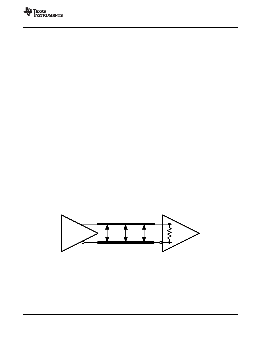
INPUT INTERFACING
The DS90LV804 accepts differential signals and allow simple AC or DC coupling. With a wide common mode
range, the DS90LV804 can be DC-coupled with all common differential drivers (that is, LVPECL, LVDS, CML).
Figure 2, Figure 3, and Figure 4 illustrate typical DC-coupled interface to common differential drivers. Note that
the DS90LV804 inputs are internally terminated with a 100
Ω resistor.
Figure 2. Typical LVDS Driver DC-Coupled Interface to DS90LV804 Input
Copyright 2005–2013, Texas Instruments Incorporated
5
Product Folder Links: DS90LV804
相關PDF資料 |
PDF描述 |
|---|---|
| VE-B3D-IX-F2 | CONVERTER MOD DC/DC 85V 75W |
| VE-B3B-IX-F1 | CONVERTER MOD DC/DC 95V 75W |
| VE-B3B-IW-F1 | CONVERTER MOD DC/DC 95V 100W |
| IDTAMB0582C1RJ8 | IC MEMORY BUFFER DIMM 655FCBGA |
| VE-J6Y-IY-F2 | CONVERTER MOD DC/DC 3.3V 33W |
相關代理商/技術參數(shù) |
參數(shù)描述 |
|---|---|
| DS90LV804TSQX | 功能描述:LVDS 接口集成電路 RoHS:否 制造商:Texas Instruments 激勵器數(shù)量:4 接收機數(shù)量:4 數(shù)據(jù)速率:155.5 Mbps 工作電源電壓:5 V 最大功率耗散:1025 mW 最大工作溫度:+ 85 C 封裝 / 箱體:SOIC-16 Narrow 封裝:Reel |
| DS90LV804TSQX/NOPB | 功能描述:LVDS 接口集成電路 RoHS:否 制造商:Texas Instruments 激勵器數(shù)量:4 接收機數(shù)量:4 數(shù)據(jù)速率:155.5 Mbps 工作電源電壓:5 V 最大功率耗散:1025 mW 最大工作溫度:+ 85 C 封裝 / 箱體:SOIC-16 Narrow 封裝:Reel |
| DS-90U | 制造商:Doublesight 功能描述:9" Smart USB LCD Monitor 制造商:DOUBLESIGHT 功能描述:9 USB LCD MONITOR USB 16:10 |
| DS90UA101-Q1 | 制造商:TI 制造商全稱:Texas Instruments 功能描述:DS90UA101-Q1 Multi-Channel Digital Audio Link |
| DS90UA101-Q1EVM | 制造商:Texas Instruments 功能描述:DS90UA101-Q1EVM - Boxed Product (Development Kits) |
發(fā)布緊急采購,3分鐘左右您將得到回復。