- 您現(xiàn)在的位置:買賣IC網(wǎng) > PDF目錄15797 > DSP56F801EVM (Freescale Semiconductor)KIT EVALUATION FOR DSP56F801 PDF資料下載
參數(shù)資料
| 型號: | DSP56F801EVM |
| 廠商: | Freescale Semiconductor |
| 文件頁數(shù): | 3/48頁 |
| 文件大小: | 0K |
| 描述: | KIT EVALUATION FOR DSP56F801 |
| 標(biāo)準(zhǔn)包裝: | 1 |
第1頁第2頁當(dāng)前第3頁第4頁第5頁第6頁第7頁第8頁第9頁第10頁第11頁第12頁第13頁第14頁第15頁第16頁第17頁第18頁第19頁第20頁第21頁第22頁第23頁第24頁第25頁第26頁第27頁第28頁第29頁第30頁第31頁第32頁第33頁第34頁第35頁第36頁第37頁第38頁第39頁第40頁第41頁第42頁第43頁第44頁第45頁第46頁第47頁第48頁
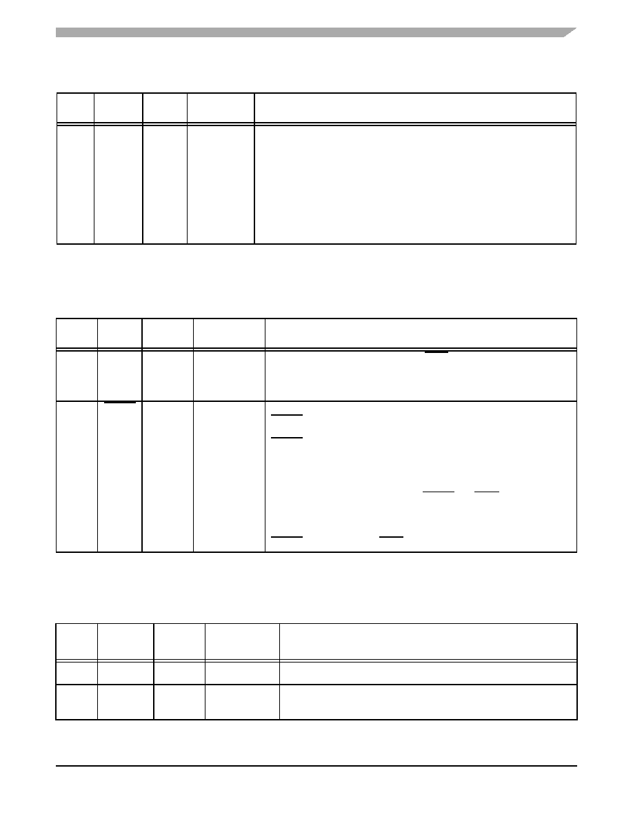
Interrupt and Program Control Signals
56F801 Technical Data, Rev. 17
Freescale Semiconductor
11
2.4 Interrupt and Program Control Signals
2.5 Pulse Width Modulator (PWM) Signals
1
XTAL
GPIOB3
Output
Input/
Output
Chip-
driven
Input
Crystal Oscillator Output—This output should be connected to an 8MHz
external crystal or ceramic resonator. For more information, please refer to
This pin can also be connected to an external clock source. For more
information, please refer to Section 3.5.3.
Port B GPIO—This multiplexed pin is a General Purpose I/O (GPIO) pin that
can be programmed as an input or output pin. This I/O can be utilized when
using the on-chip relaxation oscillator so the XTAL pin is not needed.
Table 2-6 Interrupt and Program Control Signals
No. of
Pins
Signal
Name
Signal
Type
State
During Reset
Signal Description
1
IRQA
Input
(Schmitt)
Input
External Interrupt Request A—The IRQA input is a synchronized
external interrupt request that indicates that an external device is
requesting service. It can be programmed to be level-sensitive or
negative-edge- triggered.
1
RESET
Input
(Schmitt)
Input
Reset—This input is a direct hardware reset on the processor. When
RESET is asserted low, the controller is initialized and placed in the
Reset state. A Schmitt trigger input is used for noise immunity. When the
RESET pin is deasserted, the initial chip operating mode is latched from
the EXTBOOT pin. The internal reset signal will be deasserted
synchronous with the internal clocks, after a fixed number of internal
clocks.
To ensure complete hardware reset, RESET and TRST should be
asserted together. The only exception occurs in a debugging
environment when a hardware device reset is required and it is
necessary not to reset the OnCE/JTAG module. In this case, assert
RESET, but do not assert TRST.
Table 2-7 Pulse Width Modulator (PWMA) Signals
No. of
Pins
Signal
Name
Signal
Type
State During
Reset
Signal Description
6
PWMA0-5
Output
Tri-stated
PWMA0-5— These are six PWMA output pins.
1
FAULTA0
Input
(Schmitt)
Input
FAULTA0— This fault input pin is used for disabling selected PWMA
outputs in cases where fault conditions originate off-chip.
Table 2-5 PLL and Clock (Continued)
No. of
Pins
Signal
Name
Signal
Type
State
During Reset
Signal Description
相關(guān)PDF資料 |
PDF描述 |
|---|---|
| RL187-221J-RC | INDUCTOR FIXED 220UH 5% RADIAL |
| RL187-151J-RC | INDUCTOR FIXED 150UH 5% RADIAL |
| RL187-101J-RC | INDUCTOR FIXED 100UH 5% RADIAL |
| RP20-2412DFW/N | CONV DC/DC 20W 9-36VIN +/-12VOUT |
| TC1271AMVRCTR | IC RESET MONITOR 4.38V SOT143-4 |
相關(guān)代理商/技術(shù)參數(shù) |
參數(shù)描述 |
|---|---|
| DSP56F801EVMUM | 制造商:未知廠家 制造商全稱:未知廠家 功能描述:56F801 Evaluation Module Hardware User's Manual |
| DSP56F801FA60 | 功能描述:數(shù)字信號處理器和控制器 - DSP, DSC 60Mhz/30MIPS RoHS:否 制造商:Microchip Technology 核心:dsPIC 數(shù)據(jù)總線寬度:16 bit 程序存儲器大小:16 KB 數(shù)據(jù) RAM 大小:2 KB 最大時鐘頻率:40 MHz 可編程輸入/輸出端數(shù)量:35 定時器數(shù)量:3 設(shè)備每秒兆指令數(shù):50 MIPs 工作電源電壓:3.3 V 最大工作溫度:+ 85 C 封裝 / 箱體:TQFP-44 安裝風(fēng)格:SMD/SMT |
| DSP56F801FA60E | 功能描述:數(shù)字信號處理器和控制器 - DSP, DSC 16 BIT HYBRID CONTROLLER RoHS:否 制造商:Microchip Technology 核心:dsPIC 數(shù)據(jù)總線寬度:16 bit 程序存儲器大小:16 KB 數(shù)據(jù) RAM 大小:2 KB 最大時鐘頻率:40 MHz 可編程輸入/輸出端數(shù)量:35 定時器數(shù)量:3 設(shè)備每秒兆指令數(shù):50 MIPs 工作電源電壓:3.3 V 最大工作溫度:+ 85 C 封裝 / 箱體:TQFP-44 安裝風(fēng)格:SMD/SMT |
| DSP56F801FA60E | 制造商:Freescale Semiconductor 功能描述:Digital Signal Processor IC DSP Type:Pro |
| DSP56F801FA60E | 制造商:Freescale Semiconductor 功能描述:DIGITAL SIGNAL PROCESSORLQFP3.6V |
發(fā)布緊急采購,3分鐘左右您將得到回復(fù)。
