- 您現(xiàn)在的位置:買賣IC網 > PDF目錄382961 > FM3808-70-T (Electronic Theatre Controls, Inc.) 4Kb FRAM Serial 3V Memory PDF資料下載
參數(shù)資料
| 型號: | FM3808-70-T |
| 廠商: | Electronic Theatre Controls, Inc. |
| 元件分類: | DRAM |
| 英文描述: | 4Kb FRAM Serial 3V Memory |
| 中文描述: | 4Kb的鐵電串行3V的記憶 |
| 文件頁數(shù): | 5/28頁 |
| 文件大?。?/td> | 191K |
| 代理商: | FM3808-70-T |
第1頁第2頁第3頁第4頁當前第5頁第6頁第7頁第8頁第9頁第10頁第11頁第12頁第13頁第14頁第15頁第16頁第17頁第18頁第19頁第20頁第21頁第22頁第23頁第24頁第25頁第26頁第27頁第28頁
FM3808
Rev 1.1
May 2003
Page 5 of 28
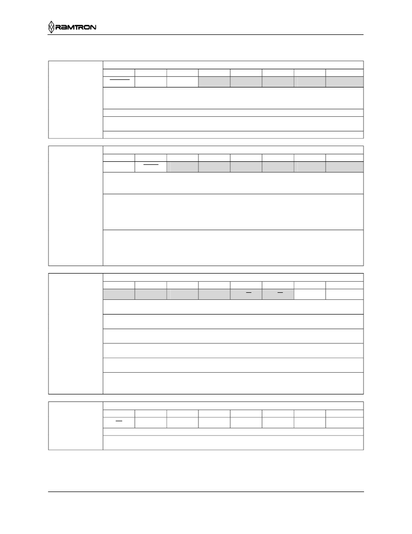
Address
7FF8h
Description
Control-Nonvolatile
D7
D6
D5
D4
D3
D2
D1
D0
OSCEN
/Oscillator Enable. When set to 1, the oscillator is halted. When set to 0, the oscillator runs. Disabling
the oscillator saves battery power during storage. On a no-battery power up, this bit is set to 1.
The
RTC will not run until the oscillator is enabled. Set this bit to 0 to activate the RTC.
Do not use. Should remain set to 0.
Calibration sign. Determines if the calibration adjustment is applied as an addition to or as a subtraction
from the time-base. This bit is implemented in FRAM. Calibration is explained below
These four bits control the calibration of the clock. These bits are implemented in FRAM.
Watchdog Timer
D7
D6
D5
D4
Reserved
Reserved
CALS
CAL.3
CAL.2
CAL.1
CAL.0
/OSCEN
Reserved
CALS
CAL.3-0
7FF7h
D3
D2
D1
D0
WDS
Watchdog Strobe. Setting this bit to 1 reloads and restarts the watchdog timer. Setting the bit to 0 has no
affect. The bit is cleared automatically once the watchdog timer is reset. The WDS bit is write only.
Reading it always will return a 0.
Watchdog Write Enable. Setting this bit to 1 masks the watchdog timeout value (WDT.5-0) so it cannot
be written. This allows the user to strobe the watchdog without disturbing the timeout value. Setting this
bit to 0 allows bits 5-0 to be written on the next write to the Watchdog register. The new value will be
loaded on the next internal watchdog clock after the write cycle is complete. This function is explained
in more detail in the watchdog Timer section below.
Watchdog Timeout selection. The watchdog timer interval is selected by the 6-bit value in this register.
It represents a multiplier of the 32 Hz count (31.25 ms). The minimum range or timeout value is 31.25
ms (a setting of 1) and the maximum timeout is 2 seconds (setting of 3Fh). Setting the watchdog timer
register to 0 disables the timer. These bits can be written only if the /WDW bit was cleared to 0 on a
previous cycle.
Interrupts
D7
D6
D5
D4
WDW
WDT.5
WDT.4
WDT.3
WDT.2
WDT.1
WDT.0
WDS
/WDW
WDT.5-0
7FF6h
D3
D2
D1
D0
WIE
AIE
PFE
ABE
H/L
P/L
Reserved
Reserved
WIE
Watchdog Interrupt Enable. When set to 1 and a watchdog timeout occurs, the watchdog timer drives
the INT pin as well as the WDF flag. When set to 0, the watchdog timeout affects only the WDF flag.
Alarm Interrupt Enable. When set to 1, the alarm match drives the INT pin as well as the AF flag. When
set to 0, the alarm match only affects the AF flag.
Power-Fail Enable. When set to 1, the power-fail monitor drives the pin as well as the PF flag. When set
to 0, the power-fail monitor affects only the PF flag.
Alarm Battery-backup Enable. When set to 1, the alarm interrupt (as controlled by AIE) will function
even in battery backup mode. When set to 0, the alarm will occur only when VDD>VLO.
High/Low. When set to a 1, the INT pin is push/pull active high. When set to a 0, the INT pin is open
drain, active low.
Pulse/Level. When set to a 1, the INT pin is driven active (determined by H/L) by an interrupt source
for approximately 200 ms. When set to a 0, the INT pin is driven to an active level (as set by H/L) until
the Flags/Control register is read.
Alarm – Date of the month
D7
D6
D5
D4
AIE
PFE
ABE
H/L
P/L
7FF5h
D3
D2
D1
D0
M
0
10 date.1
10 date.0
Date.3
Date.2
Date.1
Date.0
/M
Contains the alarm value for the date of the month and the mask bit to select or deselect the date value.
Match. Setting this bit to 0 causes the date value to be used in the alarm match. Setting this bit to 1
causes the match circuit to ignore the date value.
相關PDF資料 |
PDF描述 |
|---|---|
| FM3808DK | 4Kb FRAM Serial 3V Memory |
| FMA10A | General Purpose(Dual Digital Transistor)(通用(雙數(shù)字晶體管)) |
| FMA11A | Emitter Common (Dual Digital Transistors)(公共發(fā)射級(雙數(shù)字晶體管)) |
| FMA1 | General purpose (dual digital transistors) |
| FMA1A | General purpose (dual digital transistors) |
相關代理商/技術參數(shù) |
參數(shù)描述 |
|---|---|
| FM3808DK | 制造商:RAMTRON 制造商全稱:RAMTRON 功能描述:256Kb Bytewide FRAM w/ Real-Time Clock |
| FM3808-S | 制造商:Ramtron International Corporation 功能描述:FRAM RTC 256K SMD 3808 TSOP32 |
| FM3808-SG | 制造商:Ramtron International Corporation 功能描述:FRAM RTC 256K SMD 3808 TSOP32 |
| FM380-A | 制造商:FORMOSA 制造商全稱:Formosa MS 功能描述:Silicon epitaxial planer type |
| FM380-AL | 制造商:FORMOSA 制造商全稱:Formosa MS 功能描述:Chip Schottky Barrier Diodes - Silicon epitaxial planer type |
發(fā)布緊急采購,3分鐘左右您將得到回復。