- 您現(xiàn)在的位置:買賣IC網(wǎng) > PDF目錄382961 > FM3808 (Electronic Theatre Controls, Inc.) 4Kb FRAM Serial 3V Memory PDF資料下載
參數(shù)資料
| 型號: | FM3808 |
| 廠商: | Electronic Theatre Controls, Inc. |
| 元件分類: | DRAM |
| 英文描述: | 4Kb FRAM Serial 3V Memory |
| 中文描述: | 4Kb的鐵電串行3V的記憶 |
| 文件頁數(shù): | 20/28頁 |
| 文件大?。?/td> | 191K |
| 代理商: | FM3808 |
第1頁第2頁第3頁第4頁第5頁第6頁第7頁第8頁第9頁第10頁第11頁第12頁第13頁第14頁第15頁第16頁第17頁第18頁第19頁當(dāng)前第20頁第21頁第22頁第23頁第24頁第25頁第26頁第27頁第28頁
FM3808
Rev 1.1
May 2003
Page 20 of 28
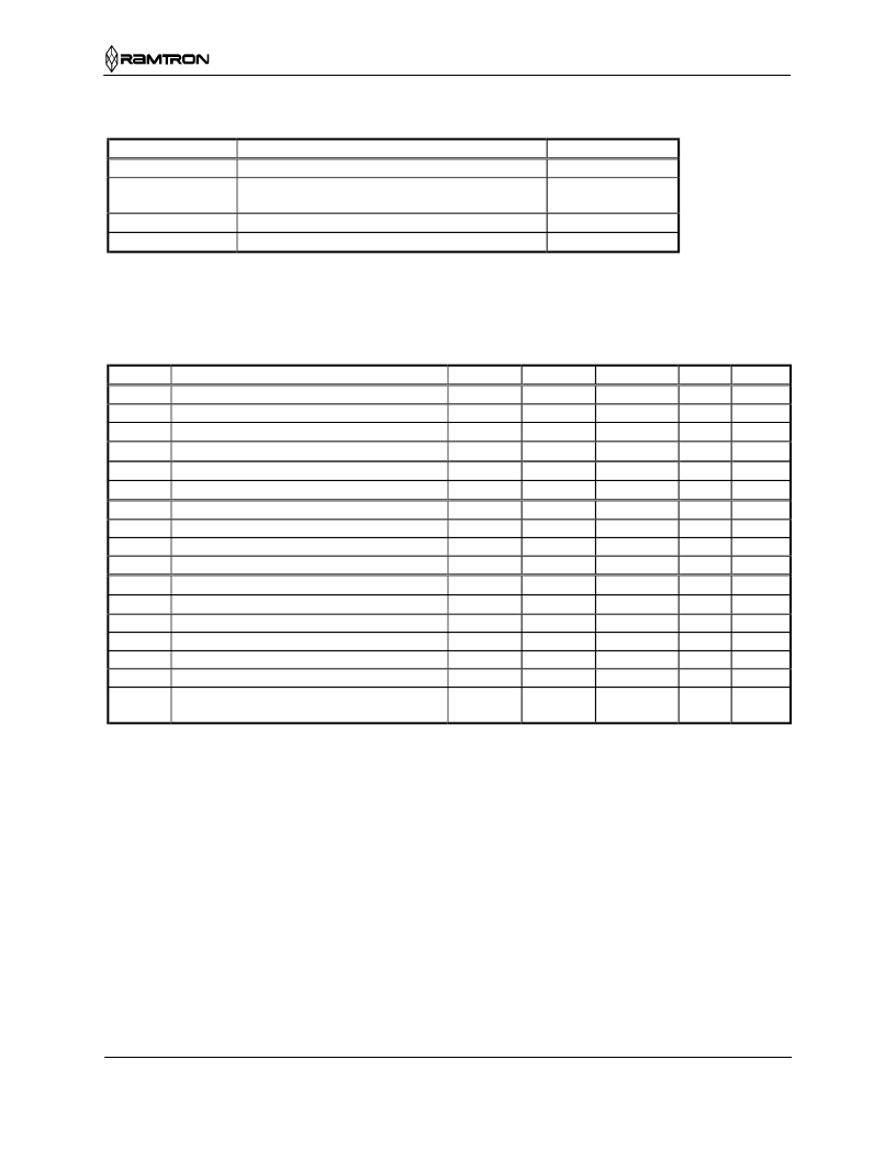
Electrical Specifications
Absolute Maximum Ratings
Symbol
V
DD
V
IN
Description
Ratings
-1.0V to +7.0V
-1.0V to +7.0V and
V
IN
< V
DD
+1.0V
-55
°
C to + 125
°
C
300
°
C
Power Supply Voltage with respect to V
SS
Voltage on any signal pin with respect to V
SS
T
STG
T
LEAD
Storage temperature
Lead temperature (Soldering, 10 seconds)
Stresses above those listed under Absolute Maximum Ratings may cause permanent damage to the device.
This is a stress rating only, and the functional operation of the device at these or any other conditions above
those listed in the operational section of this specification is not implied. Exposure to absolute maximum
ratings conditions for extended periods may affect device reliability.
DC Operating Conditions
(T
A
= -40
°
C to + 85
°
C, V
DD
= 4.5V to 5.5V unless otherwise specified)
Symbol
Parameter
V
DD
Power Supply Voltage
I
DD
V
DD
Supply Current – Active
I
SB1
Standby Current – TTL
I
SB2
Standby Current – CMOS
V
BAK
Clock Backup Voltage
I
BAK
Clock backup current
V
TP
V
DD
trip point voltage that activates INT pin
V
LO
V
DD
Lockout Voltage
V
SW
V
DD
Voltage that causes switch to V
BAK
V
RST
V
DD
Voltage for Active INT pin
I
LI
Input Leakage Current
I
LO
Output Leakage Current
V
IH
Input High Voltage
V
IL
Input Low Voltage
V
OH
Output High Voltage (I
OH
= -2.0mA)
V
OL
Output Low Voltage (I
OL
= 4.2mA)
V
OLB
Output Low Voltage (INT pin)
Device in backup mode (V
DD
<V
BAK
)
Notes
1.
V
DD
= 5.5V, /CE cycling at minimum cycle time. All inputs at CMOS levels, all outputs unloaded.
2.
V
DD
= 5.5V, /CE at V
IH
, All other inputs and DQ pins at TTL levels.
3.
V
DD
= 5.5V, /CE at V
IH
, All other inputs and DQ pins at CMOS levels.
4.
V
BAK
= 3.0V, V
DD
< V
BAK
; oscillator running. This parameter is characterized, not 100% tested.
5.
V
SW
occurs when V
DD
drops below V
BAK
. V
SW
is also the point at which the timekeeper draws current from the V
BAK
pin,
rather than from V
DD
. V
SW
is not otherwise used for control signals or functions.
6.
INT pin conditions are I
OL
= 80 uA and V
OL
= 0.4V.
7.
V
IN
, V
OUT
between V
DD
and V
SS
.
8.
Memory and register access is blocked when V
DD
< V
LO
.
9.
V
DD
=0, V
BAK
= 3.0V, I
OL
= 4.2 mA.
Min
4.5
2.5
4.35
4.2
1.2
2.0
-0.5
2.4
Typ
5.0
10
3.0
V
BAK
Max
5.5
25
500
150
V
DD
1
4.65
4.49
10
10
V
DD
+ 0.5
0.8
0.4
0.7
Units
V
mA
μ
A
μ
A
V
μ
A
V
V
V
V
μ
A
μ
A
V
V
V
V
V
Notes
1
2
3
4
8
5
6
7
7
9
相關(guān)PDF資料 |
PDF描述 |
|---|---|
| FM3808-70-T | 4Kb FRAM Serial 3V Memory |
| FM3808DK | 4Kb FRAM Serial 3V Memory |
| FMA10A | General Purpose(Dual Digital Transistor)(通用(雙數(shù)字晶體管)) |
| FMA11A | Emitter Common (Dual Digital Transistors)(公共發(fā)射級(雙數(shù)字晶體管)) |
| FMA1 | General purpose (dual digital transistors) |
相關(guān)代理商/技術(shù)參數(shù) |
參數(shù)描述 |
|---|---|
| FM3808_06 | 制造商:RAMTRON 制造商全稱:RAMTRON 功能描述:256Kb Bytewide FRAM w/ Real-Time Clock |
| FM3808-70-T | 制造商:未知廠家 制造商全稱:未知廠家 功能描述:256Kb Bytewide FRAM w/ Real-Time Clock |
| FM3808DK | 制造商:RAMTRON 制造商全稱:RAMTRON 功能描述:256Kb Bytewide FRAM w/ Real-Time Clock |
| FM3808-S | 制造商:Ramtron International Corporation 功能描述:FRAM RTC 256K SMD 3808 TSOP32 |
| FM3808-SG | 制造商:Ramtron International Corporation 功能描述:FRAM RTC 256K SMD 3808 TSOP32 |
發(fā)布緊急采購,3分鐘左右您將得到回復(fù)。