- 您現(xiàn)在的位置:買賣IC網(wǎng) > PDF目錄60231 > G1117T63U (Global Mixed-mode Technology Inc.) 1A Adjustable Low-Dropout Linear Regulator PDF資料下載
參數(shù)資料
| 型號(hào): | G1117T63U |
| 廠商: | Global Mixed-mode Technology Inc. |
| 英文描述: | 1A Adjustable Low-Dropout Linear Regulator |
| 中文描述: | 第1A可調(diào)低壓差線性穩(wěn)壓器 |
| 文件頁(yè)數(shù): | 2/9頁(yè) |
| 文件大小: | 301K |
| 代理商: | G1117T63U |
Ver: 1.9
Mar 07, 2007
TEL: 886-3-5788833
http://www.gmt.com.tw
2
G1117
Global Mixed-mode Technology Inc.
Absolute Maximum Ratings
(Note 1)
Input Voltage. . . . . . . . . . . . . . . . . . . . . . . . . . . . . . .7V
Power Dissipation Internally Limited
(Note 2)
Maximum Junction Temperature . . . . . . . . . . . . . .150°C
Reflow Temperature (soldering, 10sec) . . . . . . 260°C
Thermal Resistance Junction to Ambient, (θJA)
SOT-223 . . . . . . . . . . . . . . . . . . . . . . . . . . . .116°C/W
Thermal Resistance Junction to Case, (θJc)
SOT-223 . . . . . . . . . . . . . . . . . . . . . . . . . . . . .21°C/W
Note (1): See Recommended Minimum Footprint
Operating Conditions
(Note 1)
(VIN-VADJ) Voltage. . . . . . . . . . . . . . . . . . . . . .2.5V~6.5V
Temperature Range. . . . . . . . . . . . . .-40°C
≤ TA ≤85°C
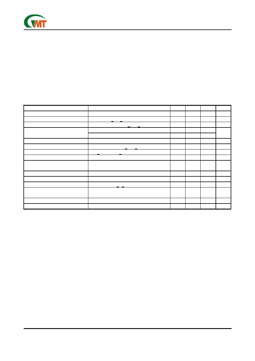
Electrical Characteristics
Operating Conditions: VIN ≤ 6.5V, TJ = 25°C unless otherwise specified. [Note3]
PARAMETER
CONDITIONS
MIN
TYP
MAX
UNITS
Reference Voltage
VIN - VOUT = 2V, IOUT = 10mA
1.225
1.250
1.275
V
Line Regulation
(VOUT + 1.5V) < VIN < 6.5V, IOUT = 10mA
---
1.32
---
%
Load Regulation
(VIN - VOUT) = 2V, 10mA < IOUT < 1A
---
0.04
---
%
ΔVOUT = 2%, IOUT = 800mA
---
1.2
1.3
Dropout Voltage
ΔVOUT = 2%, IOUT = 1A
---
1.3
1.4
V
Current Limit
(VIN - VOUT) = 2V
1000
1200
---
mA
Adjust Pin Current Change
VIN - VOUT = 2V, 10mA < IOUT < 1A
---
0.15
---
A
Minimum Load Current
1.5V < (VIN - VOUT) < 5.25V
10
---
mA
Quiescent Current
VIN - VOUT = 2V
30
80
150
A
Ripple Rejection
f = 120Hz, COUT = 10μF Tantalum,
(VIN - VOUT) = 3V, IOUT = 800mA
---
50
---
dB
Thermal Regulation
TA = 25°C, 30ms pulse
---
0.004
0.02
%/W
Temperature Stability
VIN = 4V, IO =10mA
---
0.3
---
%
RMS Output Noise (% of VOUT)
TA = 25°C, 10Hz < f < 10kHz, ILOAD = 10mA
---
0.007
---
%
Thermal Resistor Junction-to-Ambient
(No heat sink; No air flow)
SOT-223; Recommended Minimum Footprint
---
116
---
°C/W
Thermal Shutdown
Junction Temperature
---
150
---
°C
Thermal Shutdown Hysteresis
---
10
---
°C
Note1:
Absolute Maximum Ratings are limits beyond which damage to the device may occur. Operating Conditions are
conditions under which the device functions but the specifications might not be guaranteed. For guaranteed specifications
and test conditions see the Electrical Characteristics.
Note2:
The maximum power dissipation is a function of the maximum junction temperature, TJmax ; total thermal resistance, θJA,
and ambient temperature TA. The maximum allowable power dissipation at any ambient temperature is Tjmax-TA / θJA. If
this dissipation is exceeded, the die temperature will rise above 150°C and IC will go into thermal shutdown. For the
G1117 in SOT-223 package;
θJA is 116°C/W (See recommend minimum footprint).
Note3:
Low duty pulse techniques are used during test to maintain junction temperature as close to ambient as possible.
Note4:
The type of output capacitor should be tantalum or aluminum.
相關(guān)PDF資料 |
PDF描述 |
|---|---|
| G1117TD3B | 1A Adjustable Low-Dropout Linear Regulator |
| G1117 | GaAsP photodiode |
| G1118 | GaAsP photodiode |
| G1120 | GaAsP photodiode |
| G1126-02 | GaAsP photodiode |
相關(guān)代理商/技術(shù)參數(shù) |
參數(shù)描述 |
|---|---|
| G1117T63UF | 制造商:GMT 功能描述:1A Adjustable LDO |
| G1117TD3B | 制造商:GMT 制造商全稱:Global Mixed-mode Technology Inc 功能描述:1A Adjustable Low-Dropout Linear Regulator |
| G1117-XX | 制造商:GMT 制造商全稱:Global Mixed-mode Technology Inc 功能描述:1A Low-Dropout Linear Regulator |
| G1118 | 制造商:HAMAMATSU 制造商全稱:Hamamatsu Corporation 功能描述:GaAsP photodiode |
| G11190 | 功能描述:大功率LED - 單色 Green 527nm 1 Watt RoHS:否 制造商:Cree, Inc. 照明顏色:Blue 波長(zhǎng):465 nm 光強(qiáng)度: 光通量/輻射通量:500 mW 正向電流:350 mA 正向電壓:3.1 V 安裝風(fēng)格:SMD/SMT 功率額定值: 系列:XB-D 封裝:Reel |
發(fā)布緊急采購(gòu),3分鐘左右您將得到回復(fù)。