- 您現(xiàn)在的位置:買賣IC網(wǎng) > PDF目錄223860 > GS1515-CTM (Electronic Theatre Controls, Inc.) HDTV Serial Digital Reclocker PDF資料下載
參數(shù)資料
| 型號(hào): | GS1515-CTM |
| 廠商: | Electronic Theatre Controls, Inc. |
| 英文描述: | HDTV Serial Digital Reclocker |
| 中文描述: | 高清晰度電視串行數(shù)字時(shí)鐘恢復(fù)器 |
| 文件頁(yè)數(shù): | 3/17頁(yè) |
| 文件大?。?/td> | 336K |
| 代理商: | GS1515-CTM |
第1頁(yè)第2頁(yè)當(dāng)前第3頁(yè)第4頁(yè)第5頁(yè)第6頁(yè)第7頁(yè)第8頁(yè)第9頁(yè)第10頁(yè)第11頁(yè)第12頁(yè)第13頁(yè)第14頁(yè)第15頁(yè)第16頁(yè)第17頁(yè)
522 - 23 - 01
11
G
S
1
515
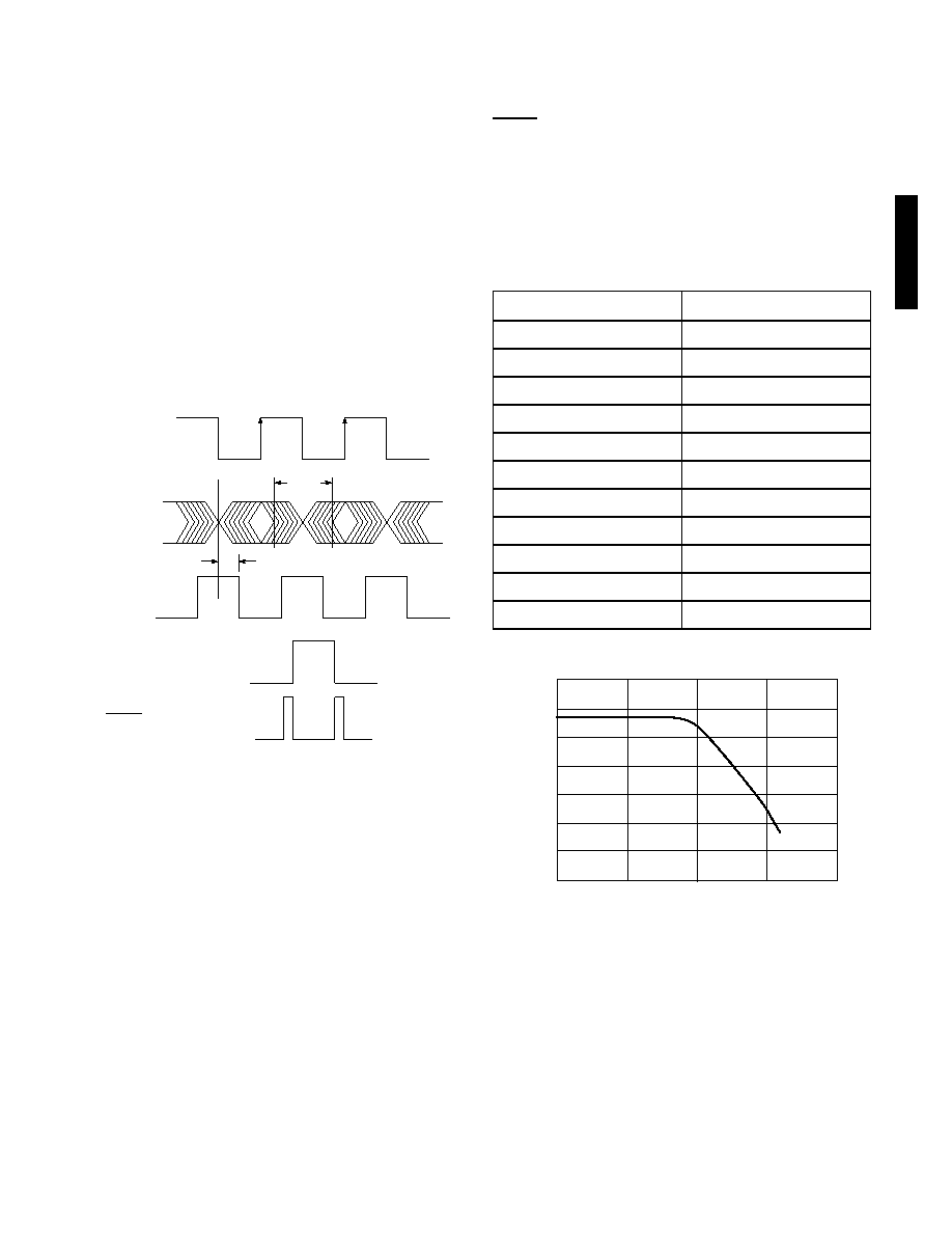
PHASE LOCK
The phase lock circuit is used to determine the phase
locked condition. It is done by generating a quadrature
clock by delaying the in-phase clock (the clock whose
falling edge is aligned to the data transition) by 166ps
(0.25UI at 1.5GHz) with the tolerance of 0.05UI. When the
PLL is locked, the falling edge of the in-phase clock is
aligned with the data edges as shown in Figure 18. The
quadrature clock is in a logic high state in the vicinity of
input data transitions. The quadrature clock is sampled and
latched by positive edges of the data transitions. The
generated signal is low pass filtered with an RC network.
The R is an on-chip 20k
resistor and C
PL is an external
capacitor (recommended value 10nF). The time constant is
about 67s, or more than a video line.
Fig. 18 PLL Circuit Principles
If the signal is not locked, the data transition phase could
be anywhere with respect to the internal clock or the
quadrature clock. In this case, the normalized filtered
sample of the quadrature clock will be 0.5. When VCO is
locked to the incoming data, data will only sample the
quadrature clock when it is logic high. The normalized
filtered sample quadrature clock will be 1.0. We chose a
threshold of 0.66 to generate the phase lock signal.
Because the threshold is lower than 1, it allows jitter to be
bigger than 0.5UI before the phase lock circuit reads it as
“not phase locked”.
INPUT JITTER INDICATOR (IJI)
This signal indicates the amount of excessive jitter (beyond
the quadrature clock window 0.5UI), which occurs beyond
the quadrature clock window
(see Figure 18). All the input
data transitions occurring outside the quadrature clock
window, will be captured and filtered by the low pass filter
as mentioned in the Phase Lock section. The running time
average of the ratio of the transitions inside the quadrature
clock and outside the quadrature is available at the PLCAP/
PLCAP pins. A signal, IJI, which is the buffered signal
available at the PLCAP is provided so that loading does not
effect the filter circuit. The signal at IJI is referenced with the
power supply such that the factor VIJI/VCC is a constant over
process
and
power
supply
for
a given input jitter
modulation. The IJI signal has 10k
output impedance.
Figure 19 shows the relationship of the IJI signal with
respect to the sine wave modulated input jitter.
Fig. 19 Input Jitter Indicator (Typical at TA = 25°C)
LOCK LOGIC
Logic is used to produce the PLL_LOCK signal which is
based on the LFS signal and phase lock signal. When there
is not any data input, the integrator will charge and
eventually saturate at either end. By sensing the saturation
of the integrator, it is determined that no data is present. If
either data is not present or phase lock is low, the lock
signal is made low. Logic signals are used to acquire the
frequency by sweeping the integrator. Injecting a current
IN-PHASE CLOCK
INPUT DATA
WITH JITTER
0.8UI
RE-TIMING
EDGE
PHASE ALIGNMENT
EDGE
QUADERATURE
CLOCK
PLCAP SIGNAL
0.25UI
P-P SINE WAVE JITTER IN UI
IJI VOLTAGE
0.00
4.75
0.15
4.75
0.30
4.75
0.39
4.70
0.45
4.60
0.48
4.50
0.52
4.40
0.55
4.30
0.58
4.20
0.60
4.10
0.63
3.95
IJI
SIGNAL
(V)
INPUT JITTER (UI)
0.00
0.20
0.40
0.60
0.80
5.0
4.8
4.6
4.4
4.2
4.0
3.8
3.6
相關(guān)PDF資料 |
PDF描述 |
|---|---|
| GS2008HET/R7 | 2 A, 800 V, SILICON, RECTIFIER DIODE |
| GS4576S09L-25 | DDR DRAM, PBGA144 |
| GS54180RK | 1 ELEMENT, 18 uH, GENERAL PURPOSE INDUCTOR, SMD |
| GS54180RJ | 1 ELEMENT, 18 uH, GENERAL PURPOSE INDUCTOR, SMD |
| GS54180BL | 1 ELEMENT, 18 uH, GENERAL PURPOSE INDUCTOR, SMD |
相關(guān)代理商/技術(shù)參數(shù) |
參數(shù)描述 |
|---|---|
| GS1522 | 制造商:GENNUM 制造商全稱:GENNUM 功能描述:HDTV Serial Digital Serializer |
| GS1522_04 | 制造商:GENNUM 制造商全稱:GENNUM 功能描述:HDTV Serial Digital Serializer |
| GS1522-CQR | 制造商:Rochester Electronics LLC 功能描述: 制造商:Gennum Corporation 功能描述: |
| GS1522-CQRE3 | 制造商:Gennum Corporation 功能描述:Monolithic Bipolar Integrated Circuit 128-Pin MQFP |
| GS1524 | 制造商:GENNUM 制造商全稱:GENNUM 功能描述:GS1524 HD-LINX-TM II Multi-Rate SDI Adaptive Cable Equalizer |
發(fā)布緊急采購(gòu),3分鐘左右您將得到回復(fù)。