- 您現(xiàn)在的位置:買賣IC網(wǎng) > PDF目錄299161 > GS8324Z36GB-250IT (GSI TECHNOLOGY) 1M X 36 ZBT SRAM, 6 ns, PBGA119 PDF資料下載
參數(shù)資料
| 型號: | GS8324Z36GB-250IT |
| 廠商: | GSI TECHNOLOGY |
| 元件分類: | SRAM |
| 英文描述: | 1M X 36 ZBT SRAM, 6 ns, PBGA119 |
| 封裝: | 14 X 22 MM, 1.27 MM PITCH, BGA-119 |
| 文件頁數(shù): | 16/46頁 |
| 文件大?。?/td> | 1157K |
| 代理商: | GS8324Z36GB-250IT |
第1頁第2頁第3頁第4頁第5頁第6頁第7頁第8頁第9頁第10頁第11頁第12頁第13頁第14頁第15頁當前第16頁第17頁第18頁第19頁第20頁第21頁第22頁第23頁第24頁第25頁第26頁第27頁第28頁第29頁第30頁第31頁第32頁第33頁第34頁第35頁第36頁第37頁第38頁第39頁第40頁第41頁第42頁第43頁第44頁第45頁第46頁
Rev: 1.00 10/2001
23/46
2001, Giga Semiconductor, Inc.
Specifications cited are subject to change without notice. For latest documentation see http://www.gsitechnology.com.
Preliminary
GS8324Z18(B/C)/GS8324Z36(B/C)/GS8324Z72(C)
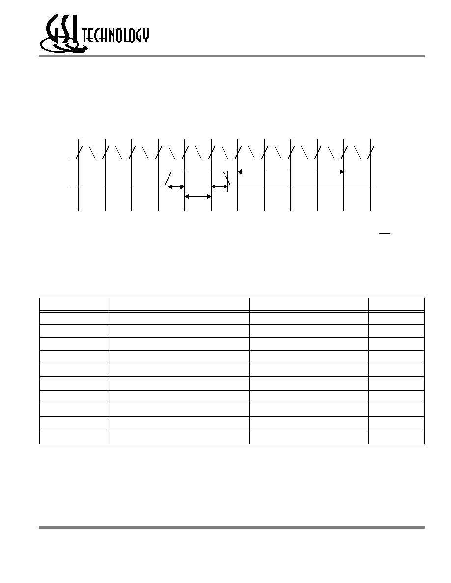
Sleep mode is dictated by the length of time the ZZ is in a High state. After entering Sleep mode, all inputs except ZZ become
disabled and all outputs go to High-Z The ZZ pin is an asynchronous, active high input that causes the device to enter Sleep mode.
When the ZZ pin is driven high, ISB2 is guaranteed after the time tZZI is met. Because ZZ is an asynchronous input, pending
operations or operations in progress may not be properly completed if ZZ is asserted. Therefore, Sleep mode must not be initiated
until valid pending operations are completed. Similarly, when exiting Sleep mode during tZZR, only a Deselect or Read commands
may be applied while the SRAM is recovering from Sleep mode.
Sleep Mode Timing Diagram
Designing for Compatibility
The GSI NBT SRAMs offer users a configurable selection between Flow Through mode and Pipeline mode via the FT signal
found on . Not all vendors offer this option, however most mark as VDD or VDDQ on pipelined parts and VSS on flow through
parts. GSI NBT SRAMs are fully compatible with these sockets.
Note:
Permanent damage to the device may occur if the Absolute Maximum Ratings are exceeded. Operation should be restricted to Recommended
Operating Conditions. Exposure to conditions exceeding the Absolute Maximum Ratings, for an extended period of time, may affect reliability of
this component.
Absolute Maximum Ratings
(All voltages reference to VSS)
Symbol
Description
Value
Unit
VDD
Voltage on VDD Pins
–
0.5 to 4.6
V
VDDQ
Voltage in VDDQ Pins
–
0.5 to 4.6
V
VCK
Voltage on Clock Input Pin
–
0.5 to 6
V
VI/O
Voltage on I/O Pins
–
0.5 to VDDQ +0.5 (≤ 4.6 V max.)
V
VIN
Voltage on Other Input Pins
–
0.5 to VDD +0.5 (≤ 4.6 V max.)
V
IIN
Input Current on Any Pin
+/–20
mA
IOUT
Output Current on Any I/O Pin
+/–20
mA
PD
Package Power Dissipation
1.5
W
TSTG
Storage Temperature
–
55 to 125
oC
TBIAS
Temperature Under Bias
–
55 to 125
oC
CK
ZZ
tZZR
tZZH
tZZS
~ ~
Sleep
相關(guān)PDF資料 |
PDF描述 |
|---|---|
| GS8324Z72GC-133IT | 512K X 72 ZBT SRAM, 10 ns, PBGA209 |
| GS840E18GB-100T | 256K X 18 CACHE SRAM, 12 ns, PBGA119 |
| GS840E18GB-180 | 256K X 18 CACHE SRAM, 8 ns, PBGA119 |
| GS8641E18F-200IT | 4M X 18 CACHE SRAM, 7.5 ns, PBGA165 |
| GS8641Z18GF-167T | 4M X 18 ZBT SRAM, 8 ns, PBGA165 |
相關(guān)代理商/技術(shù)參數(shù) |
參數(shù)描述 |
|---|---|
| GS8324Z72C200 | 制造商:G.S.I. 功能描述: |
| GS8342D06BD-350 | 制造商:GSI Technology 功能描述:165 FBGA - Bulk |
| GS8342D06BD-500 | 制造商:GSI Technology 功能描述:165 FBGA - Bulk |
| GS8342D06BD-550 | 制造商:GSI Technology 功能描述:165 FBGA - Bulk |
| GS8342D06BD-550I | 制造商:GSI Technology 功能描述:165 FBGA - Bulk |
發(fā)布緊急采購,3分鐘左右您將得到回復。