- 您現(xiàn)在的位置:買賣IC網(wǎng) > PDF目錄370389 > GS84118B-133 x18 Synchronous SRAM PDF資料下載
參數(shù)資料
| 型號: | GS84118B-133 |
| 英文描述: | x18 Synchronous SRAM |
| 中文描述: | x18同步SRAM |
| 文件頁數(shù): | 9/30頁 |
| 文件大?。?/td> | 584K |
| 代理商: | GS84118B-133 |
第1頁第2頁第3頁第4頁第5頁第6頁第7頁第8頁當(dāng)前第9頁第10頁第11頁第12頁第13頁第14頁第15頁第16頁第17頁第18頁第19頁第20頁第21頁第22頁第23頁第24頁第25頁第26頁第27頁第28頁第29頁第30頁
Rev: 1.05 7/2001
Specifications cited are subject to change without notice. For latest documentation see http://www.gsitechnology.com.
9/30
1999, Giga Semiconductor, Inc.
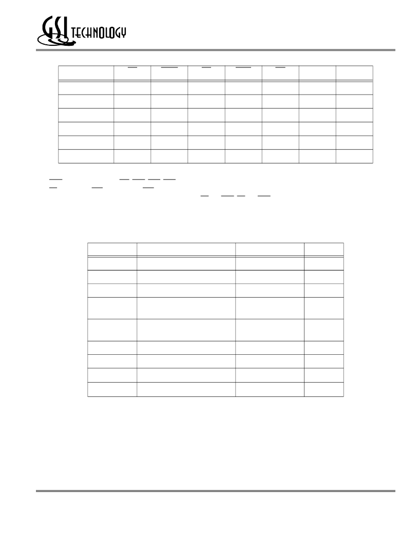
GS84118T/B-166/150/130/100
Truth Table For Read/Write/Compare/Fill Write Operation
Notes:
1.
2.
3.
4.
X means “don’t care,” H means “l(fā)ogic high,” L means “l(fā)ogic low.”
Write is the logic function of GW, BWE, BW1, BW2. See Byte Write Function table for detail.
CE is defined as CE1=L, CE2=H and CE3=L
All signals are synchronous and are sampled by CLK except OE and MOE. OE and MOE are asynchronous and drive the bus immediately.
Absolute Maximum Ratings
(Voltage reference to V
SS
= 0 V)
Symbol
Note: Permanent damage to the device may occur if the Absolute Maximun Ratings are exceeded. Functional operation should be restricted to
the recommended operation conditions. Exposure to higher than recommended voltages, for an extended period of time, could effect the
performance and reliability of this component.
CE
Write
DE
MOE
OE
Match
DQ
Read
L
H
X
X
L
—
Q
Write
L
L
L
X
H
—
D
Compare
L
H
L
L
H
Data Out
D
Fill Write
L
L
H
X
X
—
X
Match Deselect
H
X
X
L
X
High
High Z
Deselect
H
X
X
H
X
High Z
High Z
Description
Commerical
Unit
V
DD
Supply Voltage
–0.5 to 4.6
V
V
DDQ
Output Supply Voltage
–0.5 to V
DD
V
V
CLK
CLK Input Voltage
–0.5 to 6
V
V
in
Input Voltage
–0.5 to V
DD
+ 0.5
(
≤
4.6 V max. )
V
V
out
Output Voltage
–0.5 to V
DD
+ 0.5
(
≤
4.6 V max. )
V
I
out
Output Current per I/O
+/–20
mA
P
D
Power Dissipation
1.5
W
T
OPR
Operating Temperature
0 to 70
o
C
T
STG
Storage Temperature
–55 to 125
o
C
相關(guān)PDF資料 |
PDF描述 |
|---|---|
| GS84118B-150 | x18 Synchronous SRAM |
| GS84118B-166 | x18 Synchronous SRAM |
| GS84118T-100 | x18 Synchronous SRAM |
| GS84118T-133 | x18 Synchronous SRAM |
| GS84118T-150 | x18 Synchronous SRAM |
相關(guān)代理商/技術(shù)參數(shù) |
參數(shù)描述 |
|---|---|
| GS84118B-150 | 制造商:未知廠家 制造商全稱:未知廠家 功能描述:x18 Synchronous SRAM |
| GS84118B-150I | 制造商:GSI 制造商全稱:GSI Technology 功能描述:256K x 18 Sync Cache Tag |
| GS84118B-166 | 制造商:GSI 制造商全稱:GSI Technology 功能描述:256K x 18 Sync Cache Tag |
| GS84118B-166I | 制造商:GSI 制造商全稱:GSI Technology 功能描述:256K x 18 Sync Cache Tag |
| GS84118I-133I | 制造商:GSI 制造商全稱:GSI Technology 功能描述:256K x 18 Sync Cache Tag |
發(fā)布緊急采購,3分鐘左右您將得到回復(fù)。