- 您現(xiàn)在的位置:買賣IC網(wǎng) > PDF目錄371813 > HI3086JCQ (HARRIS SEMICONDUCTOR) 6-Bit, 140 MSPS, Flash A/D Converter PDF資料下載
參數(shù)資料
| 型號: | HI3086JCQ |
| 廠商: | HARRIS SEMICONDUCTOR |
| 元件分類: | ADC |
| 英文描述: | 6-Bit, 140 MSPS, Flash A/D Converter |
| 中文描述: | 1-CH 6-BIT FLASH METHOD ADC, PARALLEL ACCESS, PQFP48 |
| 文件頁數(shù): | 13/19頁 |
| 文件大小: | 215K |
| 代理商: | HI3086JCQ |
4-1418
Notes on Operation
The HI3086 is a high-speed A/D converter which is
capable of TTL, ECL and PECL level clock input. Charac-
teristic impedance should be properly matched to ensure
optimum performance during high-speed operation.
The power supply and grounding have a profound
influence on converter performance. The power supply
and grounding method are particularly important during
high-speed operation. General points for caution are as
follows:
- The ground pattern should be as large as possible. It is
recommended to make the power supply and ground
patterns wider at an inner layer using a multi-layer
board.
- To prevent interference between AGND and DGND and
between AV
CC
and DV
CC
, make sure the respective
patterns are separated. To prevent a DC offset in the
power supply pattern, connect the AV
CC
and DV
CC
lines at one point each via a ferrite-bead filter. Shorting
the AGND and DGND patterns in one place immedi-
ately under the A/D converter improves A/D converter
performance.
- Ground the power supply pins (AV
CC
, DV
CC1
, DV
CC2
,
DVEE3) as close to each pin as possible with a 0.1
μ
F or
larger ceramic chip capacitor. (Connect the AVCC pin to
the AGND pattern and the DV
CC1
, DV
CC2
, DV
EE3
pins
to the DGND pattern.)
- The digital output wiring should be as short as possible.
If the digital output wiring is long, the wiring capacitance
will increase, deteriorating the output slew rate and
resulting in reflection to the output waveform since the
original output slew rate is quite fast.
The analog input pin V
IN
has an input capacitance of
approximately 7pF. To drive the A/D converter with proper
frequency response, it is necessary to prevent perfor-
mance deterioration due to parasitic capacitance or
parasitic inductance by using a large capacity drive circuit;
keeping wiring as short as possible, and using chip parts
for resistors and capacitors, etc.
The V
RT
and V
RB
pins must have adequate bypass to
protect them from high-frequency noise. Bypass them to
AGND with approximately 1
μ
F tantal capacitor and, 0.1
μ
F
chip capacitor as short as possible.
The offset for residual is generated each for the reference
voltage pins V
RT
and V
RB
. When the offset voltage has
no influence on the IC operation, the voltage should be
applied to the V
RT
and V
RB
pins directly, keeping the
V
RBS
pin open. When the reference voltage is to be
supplied to these pins precisely, form the feedback loop
circuit with V
RT
and V
RB
as a force pin and adjust the
offset voltage to be 0V. See Figure 25 for details.
If the CLKN/E pin is not used, bypass this pin to DGND
with an approximately 0.1
μ
F capacitor. At this time,
approximately DGND3 -1.2V voltage is generated. How-
ever, this is not recommended for use as threshold voltage
V
BB
as it is too weak.
When the digital input level is ECL or PECL level, ***/E
pins should be used and ***/T pins left open. When the
digital input level is TTL, ***/T pins should be used and
***/E pins left open.
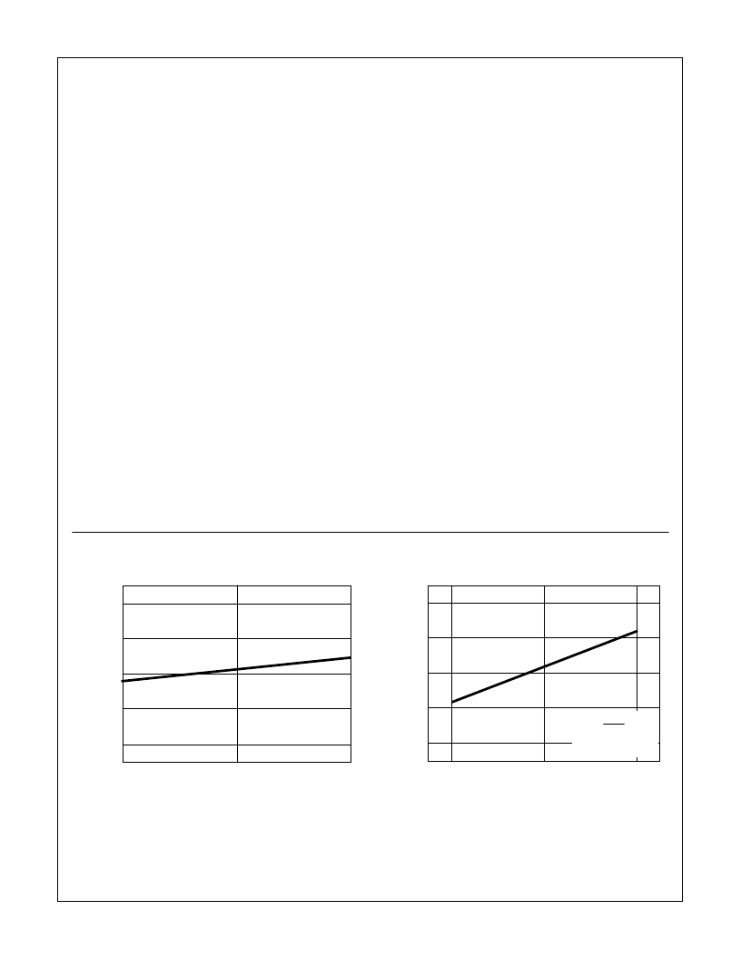
Typical Performance Curves
FIGURE 12. CURRENT CONSUMPTION vs AMBIENT
TEMPERATURE CHARACTERISTICS
FIGURE 13. CURRENT CONSUMPTION vs CONVERSION RATE
CHARACTERISTICS
70
65
60
55
50
-25
25
75
AMBIENT TEMPERATURE (
o
C)
C
50
60
70
80
90
C
0
70
140
CONVERSION RATE (MSPS)
f
CLK
4
f
IN
=
-1kHz
DEMUX MODE
C
L
= 5pF
HI3086
相關(guān)PDF資料 |
PDF描述 |
|---|---|
| HI3197JCQ | 10-Bit, 125 MSPS D/A Converter |
| HI3197 | 10-Bit, 125 MSPS D/A Converter |
| HI3276JCQ | Small glass bead with axial leads |
| HI3338KIB | TVS 6.0V 300W UNI-DIR SOT-23 |
| HI3338KIP | TVS DUAL-UNI SGL-BI 300MW SOT-23 |
相關(guān)代理商/技術(shù)參數(shù) |
參數(shù)描述 |
|---|---|
| HI3104A | 制造商:未知廠家 制造商全稱:未知廠家 功能描述:512*8 CMOS EEPROM |
| HI3104AL | 制造商:未知廠家 制造商全稱:未知廠家 功能描述:x8 EEPROM |
| HI3104AP | 制造商:未知廠家 制造商全稱:未知廠家 功能描述:x8 EEPROM |
| HI3108D | 制造商:未知廠家 制造商全稱:未知廠家 功能描述:x8 EEPROM |
| HI3108P | 制造商:未知廠家 制造商全稱:未知廠家 功能描述:x8 EEPROM |
發(fā)布緊急采購,3分鐘左右您將得到回復(fù)。