- 您現(xiàn)在的位置:買賣IC網(wǎng) > PDF目錄371896 > HSP43220JC-33 (INTERSIL CORP) CONNECTOR: SECURE DIGITAL MEMORY CARD PDF資料下載
參數(shù)資料
| 型號: | HSP43220JC-33 |
| 廠商: | INTERSIL CORP |
| 元件分類: | 數(shù)字信號處理外設(shè) |
| 英文描述: | CONNECTOR: SECURE DIGITAL MEMORY CARD |
| 中文描述: | 16-BIT, DSP-DIGITAL FILTER, PQCC84 |
| 封裝: | PLASTIC, LCC-84 |
| 文件頁數(shù): | 17/19頁 |
| 文件大小: | 190K |
| 代理商: | HSP43220JC-33 |
3-210
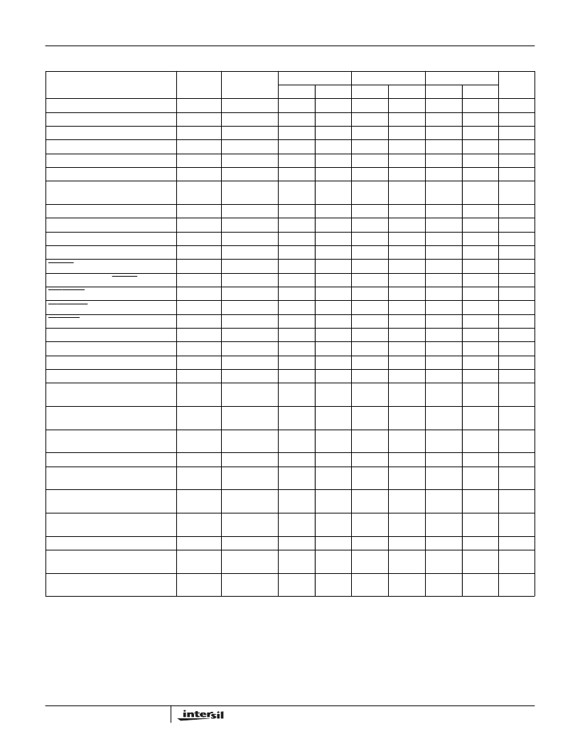
AC Electrical Specifications
V
CC
= +4.75V to +5.25V, T
A
= 0
o
C to 70
o
C
PARAMETER
SYMBOL
NOTES
-15
-25
-33
UNITS
MIN
MAX
MIN
MAX
MIN
MAX
Input Clock Frequency
F
CK
F
FIR
t
CK
t
FIR
t
SPWL
t
SPWH
t
SK
0
15
0
25.6
0
33
MHz
FIR Clock Frequency
0
15
0
25.6
0
33
MHz
Input Clock Period
66
-
39
-
30
-
ns
FIR Clock Period
66
-
39
-
30
-
ns
Clock Pulse Width Low
26
-
16
-
13
-
ns
Clock Pulse Width High
26
-
16
-
13
-
ns
Clock Skew Between FIR_CK
and CK_IN
0
t
FIR
-25
0
t
FIR
-15
0
t
FIR
-15
ns
CK_IN Pulse Width Low
t
CH1L
t
CH1H
t
CIS
t
CIH
t
RSPW
t
RTRS
t
AST
t
STOD
t
STIC
t
SET
t
HOLD
t
WL
t
WH
t
STADD
Notes 5, 8
29
-
19
-
19
-
ns
CK_IN Pulse Width High
Notes 5, 8
29
-
19
-
19
-
ns
CK_IN Setup to FIR_CK
Notes 5, 8
27
-
17
-
17
-
ns
CK_IN Hold from FIR_CK
Notes 5, 8
2
-
2
-
2
-
ns
RESET Pulse Width Low
4t
CK
8t
CK
t
CK
+10
-
-
4t
CK
8t
CK
t
CK
+10
-
-
4t
CK
8t
CK
t
CK
+10
-
-
ns
Recovery Time on RESET
-
-
-
ns
ASTARTIN Pulse Width Low
-
-
-
ns
STARTOUT Delay from CK_IN
35
20
18
ns
STARTIN Setup to CK_IN
25
-
15
-
10
-
ns
Setup Time on DATA_IN
20
-
15
-
14
-
ns
Hold Time on All inputs
0
-
0
-
0
-
ns
Write Pulse Width Low
26
-
15
-
12
-
ns
Write Pulse Width High
26
-
20
-
18
-
ns
Setup Time on Address Bus Before
the Rising Edge of Write
26
-
20
-
20
-
ns
Setup Time on Chip Select Before the
Rising Edge of Write
t
STCS
26
-
20
-
20
-
ns
SetupTimeonControlBusBeforethe
Rising Edge of Write
t
STCB
26
-
20
-
20
-
ns
DATA_RDY Pulse Width Low
t
DRPWL
t
FIRDV
2t
FIR
-20
-
-
2t
FIR
-10
-
-
2t
FIR
-10
-
-
ns
DATA_OUT Delay Relative to
FIR_CK
50
35
28
ns
DATA RDY Valid Delay Relative
to FIR_CK
t
FIRDR
-
35
-
25
-
20
ns
DATA_OUT Delay Relative to
OUT_SELH
t
OUT
-
25
-
20
-
20
ns
Output Enable to Data Out Valid
t
OEV
t
OEZ
Note 6
-
15
-
15
-
15
ns
Output Disable to Data Out
Three-State
Note 5
-
15
-
15
-
15
ns
Output Rise, Output Fall Times
t
r
, t
f
from 0.8V to
2V, Note 5
-
8
-
8
-
6
ns
NOTES:
5. Controlled by design or process parameters and not directly tested. Characterized upon initial design and after major process and/or design
changes.
6. Transition is measured at
±
200mV from steady state voltage with loading as specified in test load circuit with and C
L
= 40pF.
7. AC Testing is performed as follows: Input levels (CLK Input) 4.0V and 0V, Input levels (all other Inputs) 0V and 3.0V, Timing reference levels
(CLK) = 2.0V, (Others) = 1.5V, Output load per test load circuit and C
L
= 40pF.
8. Applies only when H_BYP = 1 or H_DRATE = 0.
HSP43220
相關(guān)PDF資料 |
PDF描述 |
|---|---|
| HSP43481GC-20 | Digital Filter |
| HSP43481GC-25 | POT 20K OHM 1/4 SQ CERM SL ST |
| HSP43481GC-30 | Digital Filter |
| HSP43481JC-20 | Digital Filter |
| HSP43481JC-25 | Digital Filter |
相關(guān)代理商/技術(shù)參數(shù) |
參數(shù)描述 |
|---|---|
| HSP43220JC-33Z | 功能描述:有源濾波器 W/ANNEAL DECIMATING DIGTL FILTER 33MHZ RoHS:否 制造商:Maxim Integrated 通道數(shù)量:1 截止頻率:150 KHz 電源電壓-最大:11 V 電源電壓-最小:4.74 V 最大工作溫度:+ 85 C 安裝風(fēng)格:Through Hole 封裝 / 箱體:PDIP N 封裝:Tube |
| HSP43220TM-15 | 制造商:未知廠家 制造商全稱:未知廠家 功能描述:Digital Filter |
| HSP43220TM-25 | 制造商:未知廠家 制造商全稱:未知廠家 功能描述:Digital Filter |
| HSP43220VC-25 | 制造商:Rochester Electronics LLC 功能描述:- Bulk 制造商:Harris Corporation 功能描述: |
| HSP43220VC-33 | 制造商:Rochester Electronics LLC 功能描述:- Bulk |
發(fā)布緊急采購,3分鐘左右您將得到回復(fù)。