- 您現(xiàn)在的位置:買賣IC網(wǎng) > PDF目錄385432 > HYB18H512321BF (QIMONDA) 512-Mbit GDDR3 Graphics RAM PDF資料下載
參數(shù)資料
| 型號(hào): | HYB18H512321BF |
| 廠商: | QIMONDA |
| 英文描述: | 512-Mbit GDDR3 Graphics RAM |
| 中文描述: | 512兆GDDR3顯卡內(nèi)存 |
| 文件頁數(shù): | 35/43頁 |
| 文件大?。?/td> | 1344K |
| 代理商: | HYB18H512321BF |
第1頁第2頁第3頁第4頁第5頁第6頁第7頁第8頁第9頁第10頁第11頁第12頁第13頁第14頁第15頁第16頁第17頁第18頁第19頁第20頁第21頁第22頁第23頁第24頁第25頁第26頁第27頁第28頁第29頁第30頁第31頁第32頁第33頁第34頁當(dāng)前第35頁第36頁第37頁第38頁第39頁第40頁第41頁第42頁第43頁
HYB18H512321BF
512-Mbit GDDR3
Internet Data Sheet
Rev. 1.1, 2007-09
05292007-WAU2-UU95
35
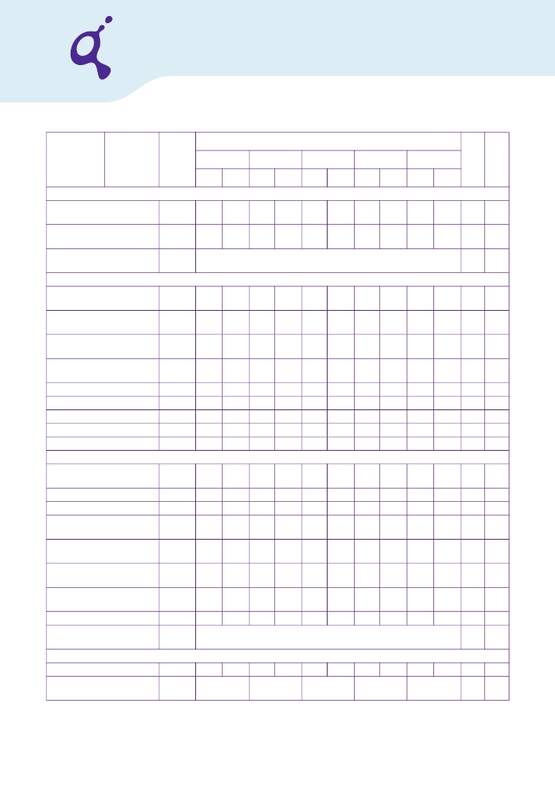
Column Timing
CAS(a) to CAS(b) Command
period
Write to Read Command
Delay
Read to Write command
delay
Write Cycle Timing Parameters for Data and Data Strobe
Write command to first
WDQS latching transition
Data-in and Data Mask to
WDQS Setup Time
Data-in and Data Mask to
WDQS Hold Time
Data-in and DM input pulse
width (each input)
DQS input low pulse width
DQS input high pulse width
DQS Write Preamble Time
DQS Write Postamble Time
Write Recovery Time
Read Cycle Timing Parameters for Data and Data Strobe
Data Access Time from
Clock
Read Preamble
t
RPRE
Read Postamble
t
RPST
Data-out high impedance
time from CLK
Data-out low impedance time
from CLK
DQS edge to Clock edge
skew
DQS edge to output data
edge skew
Data hold skew factor
t
QHS
Data output hold time from
DQS
Refresh/Power Down Timing
Refresh Period (8192 cycles)
t
REF
Average periodic Auto
Refresh interval
t
CCD
2
—
2
—
2
—
2
—
2
—
t
CK
7)
t
WTR
8
—
7
—
6
—
6
—
5
—
t
CK
8)
t
RTW
t
RTW(min)
= (CL + BL/2 +2 -WL)
t
CK
9)
t
DQSS
WL–
0.25
0.13
WL+
0.25
—
WL–
0.25
0.14
WL+
0.25
—
WL–
0.25
0.15
WL+
0.25
—
WL–
0.25
0.16
WL+
0.25
—
WL–
0.25
0.18
WL+
0.25
—
t
CK
t
DS
ns
t
DH
0.13
—
0.14
—
0.15
—
0.16
—
0.18
—
ns
t
DIPW
0.4
—
0.40
—
0.40
—
0.40
—
0.40
—
t
CK
t
DQSL
t
DQSH
t
WPRE
t
WPST
t
WR
0.45
0.45
0.75
0.75
13
—
—
1.25
1.25
—
0.40
0.40
0.75
0.75
13
—
—
1.25
1.25
—
0.40
0.40
0.75
0.75
13
—
—
1.25
1.25
—
0.40
0.40
0.75
0.75
12
—
—
1.25
1.25
—
0.40
0.40
0.75
0.75
10
—
—
1.25
1.25
—
t
CK
t
CK
t
CK
t
CK
t
CK
t
AC
-0.20 -0.20
-0.21 0.21
-0.22 0.22
-0.22 0.22
–0.25 0.25
ns
0.75
0.75
t
ACmin
t
ACmax
t
ACmin
t
ACmax
t
ACmin
t
ACmax
t
ACmin
t
ACmax
t
ACmin
t
ACmax
ns
1.25
1.25
0.75
0.75
1.25
1.25
0.75
0.75
1.25
1.25
0.75
0.75
1.25
1.25
0.75
0.75
1.25
1.25
t
CK
t
CK
t
HZ
t
LZ
t
ACmin
t
ACmax
t
ACmin
t
ACmax
t
ACmin
t
ACmax
t
ACmin
t
ACmax
t
ACmin
t
ACmax
ns
t
DQSCK
-0.20 0.20
-0.21 0.21
-0.22 0.22
-0.22 0.22
–0.25 0.25
ns
t
DQSQ
—
0.110 —
0.120 —
0.130 —
0.140 —
0.160 ns
10)
—
0.110 —
0.120 —
0.130 —
t
HP
–
t
QHS
0.140 —
0.160 ns
t
QH
ns
—
3.9
32
—
3.9
32
—
3.9
32
—
3.9
32
—
3.9
32
ms
μ
s
t
REFI
Parameter
CAS latency Symbol
Limit Values
Unit Note
-8
–10
–11
–12
–14
Min
Max
Min.
Max.
Min.
Max.
Min.
Max.
Min.
Max.
相關(guān)PDF資料 |
PDF描述 |
|---|---|
| HYB18L128160BF | DRAMs for Mobile Applications 128-Mbit Mobile-RAM |
| HYB18L256160B | DRAMs for Mobile Applications 256-Mbit Mobile-RAM |
| HYMP112S64LMP8-C4 | DDR2 SDRAM SO-DIMM |
| HYMP112S64LMP8-C5 | DDR2 SDRAM SO-DIMM |
| HYMP112S64LMP8-E3 | BNC FEMALE TO RCA MALE COUPLER |
相關(guān)代理商/技術(shù)參數(shù) |
參數(shù)描述 |
|---|---|
| HYB18H512321BF-08/10 | 制造商:QIMONDA 制造商全稱:QIMONDA 功能描述:512-Mbit GDDR3 Graphics RAM |
| HYB18H512321BF-11/12/14 | 制造商:QIMONDA 制造商全稱:QIMONDA 功能描述:512-Mbit GDDR3 Graphics RAM |
| HYB18L128160BC-7.5 | 制造商:QIMONDA 制造商全稱:QIMONDA 功能描述:DRAMs for Mobile Applications 128-Mbit Mobile-RAM |
| HYB18L128160BC-75 | 制造商:INFINEON 制造商全稱:Infineon Technologies AG 功能描述:DRAMs for Mobile Applications |
| HYB18L128160BF | 制造商:QIMONDA 制造商全稱:QIMONDA 功能描述:DRAMs for Mobile Applications 128-Mbit Mobile-RAM |
發(fā)布緊急采購,3分鐘左右您將得到回復(fù)。