- 您現(xiàn)在的位置:買賣IC網(wǎng) > PDF目錄67681 > IBM25403GCX-3JC76C2 RISC PROCESSOR, PQFP16 PDF資料下載
參數(shù)資料
| 型號: | IBM25403GCX-3JC76C2 |
| 元件分類: | 微控制器/微處理器 |
| 英文描述: | RISC PROCESSOR, PQFP16 |
| 封裝: | PLASTIC, QFP-160 |
| 文件頁數(shù): | 6/54頁 |
| 文件大小: | 541K |
| 代理商: | IBM25403GCX-3JC76C2 |
第1頁第2頁第3頁第4頁第5頁當前第6頁第7頁第8頁第9頁第10頁第11頁第12頁第13頁第14頁第15頁第16頁第17頁第18頁第19頁第20頁第21頁第22頁第23頁第24頁第25頁第26頁第27頁第28頁第29頁第30頁第31頁第32頁第33頁第34頁第35頁第36頁第37頁第38頁第39頁第40頁第41頁第42頁第43頁第44頁第45頁第46頁第47頁第48頁第49頁第50頁第51頁第52頁第53頁第54頁
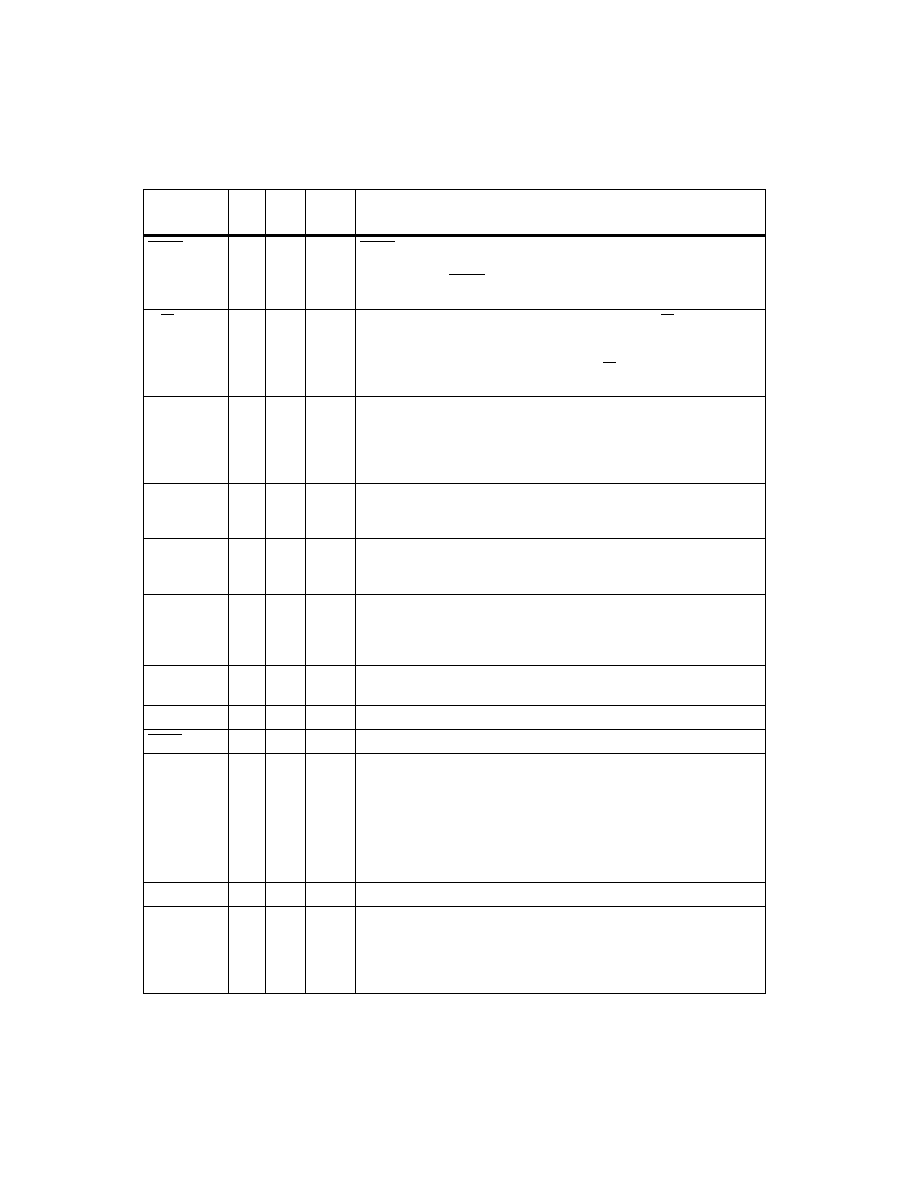
IBM PowerPC 403GCX
14
Reset
91
K14
I/O
Reset. A logic 0 input placed on this pin for one SysClk cycle
causes the 403GCX to begin a system reset. When a system reset
is invoked, the Reset pin becomes a logic 0 output for 2048 SysClk
cycles.
R/W
127
C11
I/O
Read / Write. When the 403GCX is bus master, R/W is an output
which is high when data is read from memory and low when data is
written to memory.
When the 403GCX is not bus master, R/W is an input from the
external bus master which indicates the direction of data transfer.
SerClk
26
J1
I
Serial Port Clock. Through the Serial Port Clock Source bit in the
Input/Output Conguration register (IOCR), users may choose the
serial port clock source from either the input on the SerClk pin or
processor SysClk. The maximum allowable input frequency into
SerClk is half the SysClk frequency.
SysClk
22
G3
I
SysClk is the processor system clock input. The 403GCX can also
be programmed to operate at a 2X internal clock rate while the
external bus interface runs at the SysClk input rate.
TCK
6
D2
I
JTAG Test Clock Input. TCK is the clock source for the 403GCX test
access port (TAP). The maximum clock rate into the TCK pin is one
half of the processor SysClk clock rate.
TDI
8
D1
I
Test Data In. The TDI is used to input serial data into the TAP. When
the TAP enables the use of the TDI pin, the TDI pin is sampled on
the rising edge of TCK and this data is input to the selected TAP
shift register.
TDO
16
F3
O
Test Data Output. TDO is used to transmit data from the 403GCX
TAP. Data from the selected TAP shift register is shifted out on TDO.
TestA
23
H1
I
Reserved for manufacturing test. Tied low for normal operation.
TestB
24
H2
I
Reserved for manufacturing test. Tied high for normal operation.
TestC/Hold-
Pri
37
M1
I
TestC. Reserved for manufacturing test during the reset interval.
While Reset is active, this signal should be tied low for normal oper-
ation.
HoldReq Priority. When Reset is not active, this signal is sampled to
determine the priority of the external bus master signal HoldReq. If
HoldPri = 0 then the HoldReq signal is considered high priority, oth-
erwise HoldReq is considered low priority.
TestD
38
M3
I
Reserved for manufacturing test. Tied low for normal operation.
TimerClk
25
H4
I
Timer Facility Clock. Through the Timer Clock Source bit in the
Input/Output Conguration register (IOCR), users may choose the
clock source for the Timer facility from either the input on the Timer-
Clk pin or processor CoreClk. The maximum input frequency into
TimerClk is half the CoreClk frequency.
Table 4. 403GCX Signal Descriptions
Signal
Name
Pin
Ball
I/O
Type
Function
相關(guān)PDF資料 |
PDF描述 |
|---|---|
| IBM25405GP-3BA200C2 | RISC PROCESSOR, PBGA456 |
| IBM25EMPPC603EFG-100 | 32-BIT, 100 MHz, RISC PROCESSOR, PQFP240 |
| IBM25EMPPC603EBG-100 | 32-BIT, 100 MHz, RISC PROCESSOR, CBGA255 |
| IBM25EMPPC740LDBC4000 | 32-BIT, 400 MHz, RISC PROCESSOR, CBGA255 |
| IBM25EMPPC750LCBF3330 | 32-BIT, 333 MHz, RISC PROCESSOR, CBGA360 |
相關(guān)代理商/技術(shù)參數(shù) |
參數(shù)描述 |
|---|---|
| IBM25403GCX-JA50C2 | 制造商:IBM 功能描述:403GCX-JA50C |
| IBM25403GCX-JA60C2 | 制造商:IBM 功能描述:403GCX-JA60C2 |
| IBM25C710AB3A100 | 制造商:未知廠家 制造商全稱:未知廠家 功能描述:Controller Miscellaneous - Datasheet Reference |
| IBM25CPC700BB3B66 | 制造商:未知廠家 制造商全稱:未知廠家 功能描述:Peripheral (Multifunction) Controller |
| IBM25CPC700BB3B83 | 制造商:未知廠家 制造商全稱:未知廠家 功能描述:Peripheral (Multifunction) Controller |
發(fā)布緊急采購,3分鐘左右您將得到回復。