- 您現(xiàn)在的位置:買賣IC網 > PDF目錄360784 > ICS9248YF-96-T Frequency Generator & Integrated Buffers for Celeron & PII/III⑩ PDF資料下載
參數(shù)資料
| 型號: | ICS9248YF-96-T |
| 英文描述: | Frequency Generator & Integrated Buffers for Celeron & PII/III⑩ |
| 中文描述: | 頻率發(fā)生器 |
| 文件頁數(shù): | 2/12頁 |
| 文件大?。?/td> | 206K |
| 代理商: | ICS9248YF-96-T |
2
ICS9248-96
0311D—04/23/04
General Description
Pin Configuration
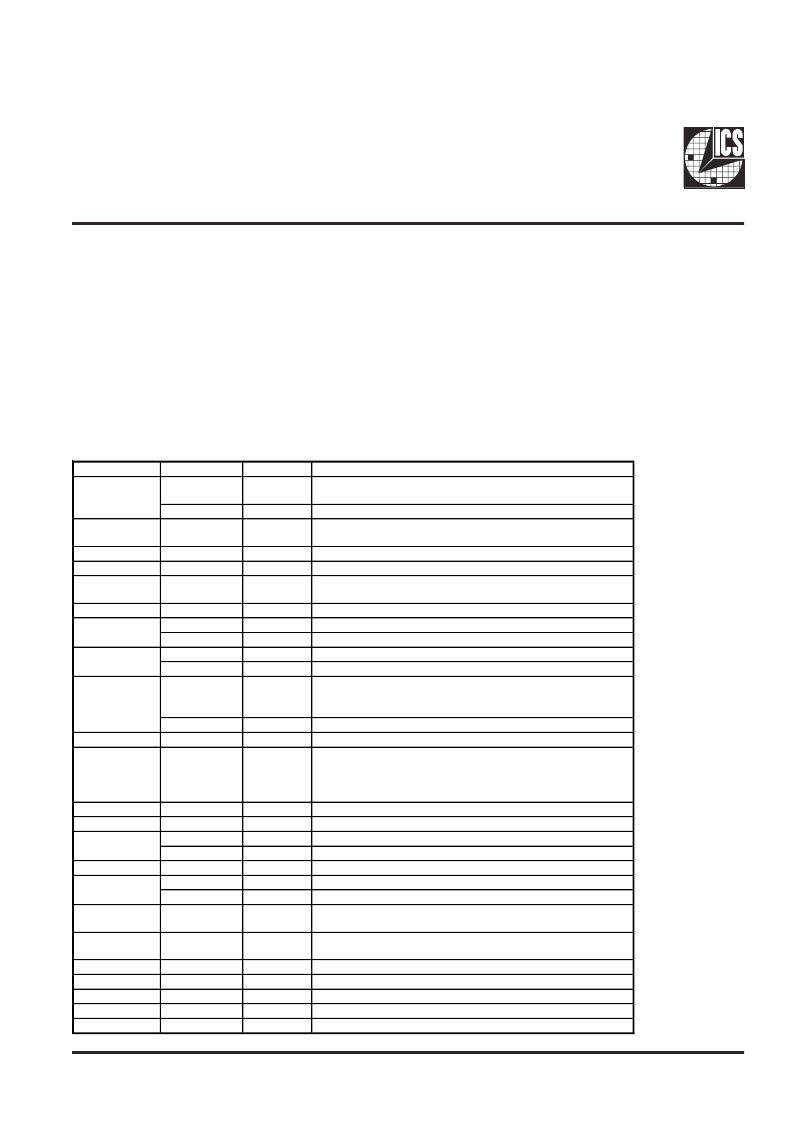
PIN NUMBER
PIN NAME
TYPE
DESCRIPTION
FREQ_IOAPIC
IN
If FREQ_APIC = 0, APIC Clock = PCICLK
If FREQ_APIC = 1, APIC Clock = PCICLK/2 (default)
14.318 MHz reference clock.
3.3V Power supply for SDRAM output buffers, PCI output buffers,
reference output buffers and 48MHz output
Crystal input,nominally 14.318MHz.
Crystal output, nominally 14.318MHz.
REF0
OUT
2, 9, 10, 18, 25,
30, 38
3
4
5, 6, 14, 21, 29,
34, 42
8, 7
VDD
PWR
X1
X2
IN
OUT
GND
PWR
Ground pin for 3V outputs.
3V66 [1:0]
FS0
PCICLK0
FS1
PCICLK1
OUT
IN
OUT
IN
OUT
3.3V Clocks
Frequency select pin.
PCI clock output
Frequency select pin.
PCI clock output
Logic inputs frequency select I/O/USB output,
When a "0" is latched, output frequency = 48MHz
When a "1" is latched, output frequency = 24MHz
PCI clock output
PCI clock outputs.
Asynchronous active low input pin used to power down the device
into a low power state. The internal clocks are disabled and the
VCO and the crystal are stopped. The latency of the power down will
not be greater than 3ms.
Clock input of I2C input, 5V tolerant input
Data input for I2C serial input, 5V tolerant input
Frequency select pin.
48MHz output clocks
48MHz output clocks
Frequency select pin.
24 or 48MHz output
Free running SDRAM - used for feed back to chipset, should remain
on always.
SEL24_48MHz#
IN
PCICLK2
PCICLK [7:3]
OUT
OUT
20, 19, 17, 16, 15
22
PD#
IN
23
24
SCLK
SDATA
FS3
48MHz_0
48MHz_1
FS2
24_48MHz
IN
IN
IN
OUT
OUT
IN
OUT
27
31
SDRAM_F
OUT
32, 33, 35, 36, 37,
39, 40, 41,
43
46
47
48
SDRAM [7:0]
OUT
SDRAM clock outputs
GNDLCPU
CPUCLK [1:0]
VDDLCPU
IOAPIC
VDDLAPIC
PWR
OUT
PWR
OUT
PWR
Ground pin for the CPU clocks.
CPU clock outputs.
Power pin for the CPUCLKs. 2.5V
2.5V clock output
Power pin for the IOAPIC. 2.5V
1
26
28
11
12
13
Power Groups
GNDREF, VDDREF = REF0, X1, X2
GNDPCI , VDDPCI = PCICLK [9:0]
GNDSDR, VDDSDR = SDRAM [7:0], SDRAM_F,
supply for PLL core
GND3V66 , VDD3V66 = 3V66
GND48 , VDD48 = 48MHz, 24_48MHz,
VDDLAPIC = IOAPIC
GNDLCPU , VDDLCPU = CPUCLK [1:0]
ICS9248-96
is the single chip clock solution for designs
using the 810/810E style chipset. It provides all necessary
clock signals for such a system.
Spread spectrum may be enabled through I
2
C
programming.
Spread spectrum typically reduces system EMI by 8dB to
10dB. This simplifies EMI qualification without resorting
to board design iterations or costly shielding. The ICS9248-
96 employs a proprietary closed loop design, which tightly
controls the percentage of spreading over process and
temperature variations.
Serial programming I
2
C interface allows changing functions,
stop clock programming and frequency selection.
相關PDF資料 |
PDF描述 |
|---|---|
| ICS932S202 | Frequency Timing Generator for Differential PIIIType Dual-CPU Systems |
| ICS932S208 | Programmable Timing Control Hub⑩ for Next Gen P4⑩ processor |
| ICS932S208YFLF-T | Programmable Timing Control Hub⑩ for Next Gen P4⑩ processor |
| ICS932S208YGLF-T | Programmable Timing Control Hub⑩ for Next Gen P4⑩ processor |
| ICS932S203 | Frequency Generator with 133MHz Differential CPU Clocks |
相關代理商/技術參數(shù) |
參數(shù)描述 |
|---|---|
| ICS9248YF-97-T | 制造商:ICS 制造商全稱:ICS 功能描述:Frequency Timing Generator for PENTIUM II Systems |
| ICS9248YF-98-T | 制造商:ICS 制造商全稱:ICS 功能描述:Frequency Generator & Integrated Buffers for Celeron & PII/III⑩ |
| ICS9248YF-99 | 制造商:ICS 制造商全稱:ICS 功能描述:Frequency Generator & Integrated Buffers for Celeron & PII/III⑩ |
| ICS9248YG-101-T | 制造商:ICS 制造商全稱:ICS 功能描述:Frequency Generator & Integrated Buffers for PENTIUM/ProTM & K6 |
| ICS9248YG-143-T | 制造商:ICS 制造商全稱:ICS 功能描述:Frequency Generator & Integrated Buffers for PENTIUM II/IIITM & K6 |
發(fā)布緊急采購,3分鐘左右您將得到回復。