- 您現(xiàn)在的位置:買賣IC網(wǎng) > PDF目錄377480 > IDT54FCT388915T70PY (INTEGRATED DEVICE TECHNOLOGY INC) 3.3V LOW SKEW PLL-BASED CMOS CLOCK DRIVER WITH (3-STATE) PDF資料下載
參數(shù)資料
| 型號(hào): | IDT54FCT388915T70PY |
| 廠商: | INTEGRATED DEVICE TECHNOLOGY INC |
| 元件分類: | 時(shí)鐘及定時(shí) |
| 英文描述: | 3.3V LOW SKEW PLL-BASED CMOS CLOCK DRIVER WITH (3-STATE) |
| 中文描述: | FCT SERIES, PLL BASED CLOCK DRIVER, 7 TRUE OUTPUT(S), 1 INVERTED OUTPUT(S), PDSO28 |
| 封裝: | 5.30 MM, 0.65 MM PITCH, SSOP-28 |
| 文件頁(yè)數(shù): | 7/11頁(yè) |
| 文件大小: | 145K |
| 代理商: | IDT54FCT388915T70PY |
IDT54/74FCT388915T 70/100/133/150
3.3V LOW SKEW PLL-BASED CLOCK DRIVER
MILITARY AND COMMERCIAL TEMPERATURE RANGES
9.8
7
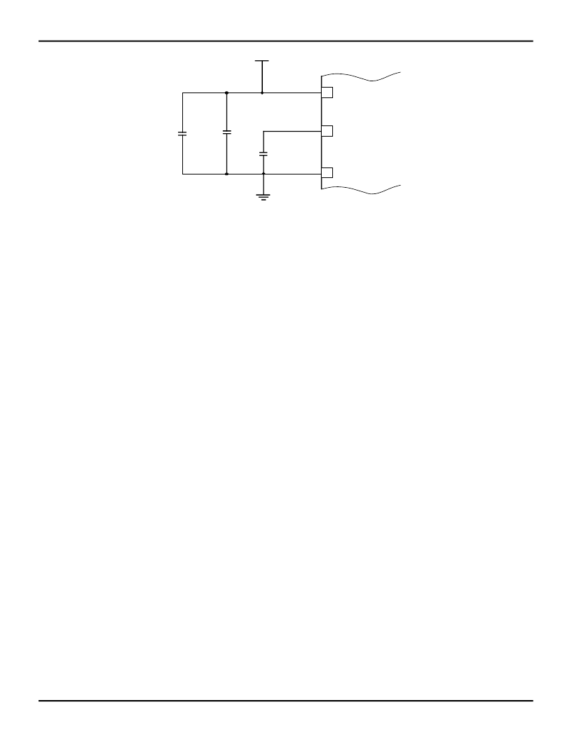
Figure 2. Recommended Loop Filter and Analog Isolation Scheme for the FCT388915T
NOTES:
1. Figure 2 shows a loop filter and analog isolation scheme which will be effective in most applications. The following guidelines should be followed to ensure
stable and jitter-free operation:
a.
All loop filter and analog isolation components should be tied as close to the package as possible. Stray current passing through the parasitics of
long traces can cause undesirable voltage transients at the LF pin.
The 10
μ
F low frequency bypass capacitor and the 0.1
μ
F high frequency bypass capacitor form a wide bandwidth filter that will minimize the
388915T's sensitivity to voltage transients from the system digital V
CC
supply and ground planes.
If good bypass techniques are used on a board design near components which may cause digital V
CC
and ground noise, V
CC
step deviations should
not occur at the 388915T's digital V
CC
supply. The purpose of the bypass filtering scheme shown in figure 2 is to give the 388915T additional
protection from the power supply and ground plane transients that can occur in a high frequency, high speed digital system.
The loop filter capacitor (0.1
μ
F) can be a ceramic chip capacitor, the same as a standard bypass capacitor.
2. In addition to the bypass capacitors used in the analog filter of figure 2 there should be a 0.1
μ
F bypass capacitor between each of the other (digital) four
V
CC
pins and the board ground plane. This will reduce output switching noise caused by the 388915T outputs, in addition to reducing potential for noise
in the "analog" section of the chip. These bypass capacitors should also be tied as close to the 388915T package as possible.
b.
c.
BOARD V
CC
0.1
μ
F (Loop
Filter Cap)
Analog loop filter
section of the
FCT388915T
0.1
μ
F
High
Freq.
Bypass
10
μ
F
Low
Freq.
Bypass
BOARD GND
ANALOG V
CC
ANALOG GND
LF
A separate Analog power supply
is not necessary and should not
be used. Following these
prescribed guidelines is all that is
necessary to use the FCT388915
in a normal digital environment.
3052 drw 12
相關(guān)PDF資料 |
PDF描述 |
|---|---|
| IDT74FCT388915T70PY | 3.3V LOW SKEW PLL-BASED CMOS CLOCK DRIVER WITH (3-STATE) |
| IDT54FCT388915T70PYB | 3.3V LOW SKEW PLL-BASED CMOS CLOCK DRIVER WITH (3-STATE) |
| IDT74FCT388915T70PYB | 3.3V LOW SKEW PLL-BASED CMOS CLOCK DRIVER WITH (3-STATE) |
| IDT74FCT807BTPYG | FAST CMOS 1-TO-10 CLOCK DRIVER |
| IDT74FCT807BTPYGI | FAST CMOS 1-TO-10 CLOCK DRIVER |
相關(guān)代理商/技術(shù)參數(shù) |
參數(shù)描述 |
|---|---|
| IDT54FCT521ADB | 制造商:Integrated Device Technology Inc 功能描述: |
| IDT54FCT533DB | 制造商:Integrated Device Technology Inc 功能描述: |
| IDT54FCT543ADB | 制造商:MAJOR 功能描述: |
| IDT54FCT543ATDB | 制造商:MAJOR 功能描述: |
| IDT54FCT573ADB | 制造商:Integrated Device Technology Inc 功能描述: |
發(fā)布緊急采購(gòu),3分鐘左右您將得到回復(fù)。