- 您現(xiàn)在的位置:買賣IC網(wǎng) > PDF目錄377340 > IDT71V3548S133PFI (INTEGRATED DEVICE TECHNOLOGY INC) 256K x 18 3.3V Synchronous ZBT SRAM 3.3V I/O, Burst Counter Pipelined Outputs PDF資料下載
參數(shù)資料
| 型號: | IDT71V3548S133PFI |
| 廠商: | INTEGRATED DEVICE TECHNOLOGY INC |
| 元件分類: | DRAM |
| 英文描述: | 256K x 18 3.3V Synchronous ZBT SRAM 3.3V I/O, Burst Counter Pipelined Outputs |
| 中文描述: | 256K X 18 ZBT SRAM, 4.2 ns, PQFP100 |
| 封裝: | 14 X 20 MM, 1.40 MM HEIGHT, PLASTIC, TQFP-100 |
| 文件頁數(shù): | 2/26頁 |
| 文件大?。?/td> | 494K |
| 代理商: | IDT71V3548S133PFI |
第1頁當(dāng)前第2頁第3頁第4頁第5頁第6頁第7頁第8頁第9頁第10頁第11頁第12頁第13頁第14頁第15頁第16頁第17頁第18頁第19頁第20頁第21頁第22頁第23頁第24頁第25頁第26頁
6.42
IDT71V3548, 256K x 18, 3.3V Synchronous SRAMS with
ZBT
Feature, 3.3V I/O, Burst Counter, and Pipelined Outputs Commercial and Industrial Temperature Ranges
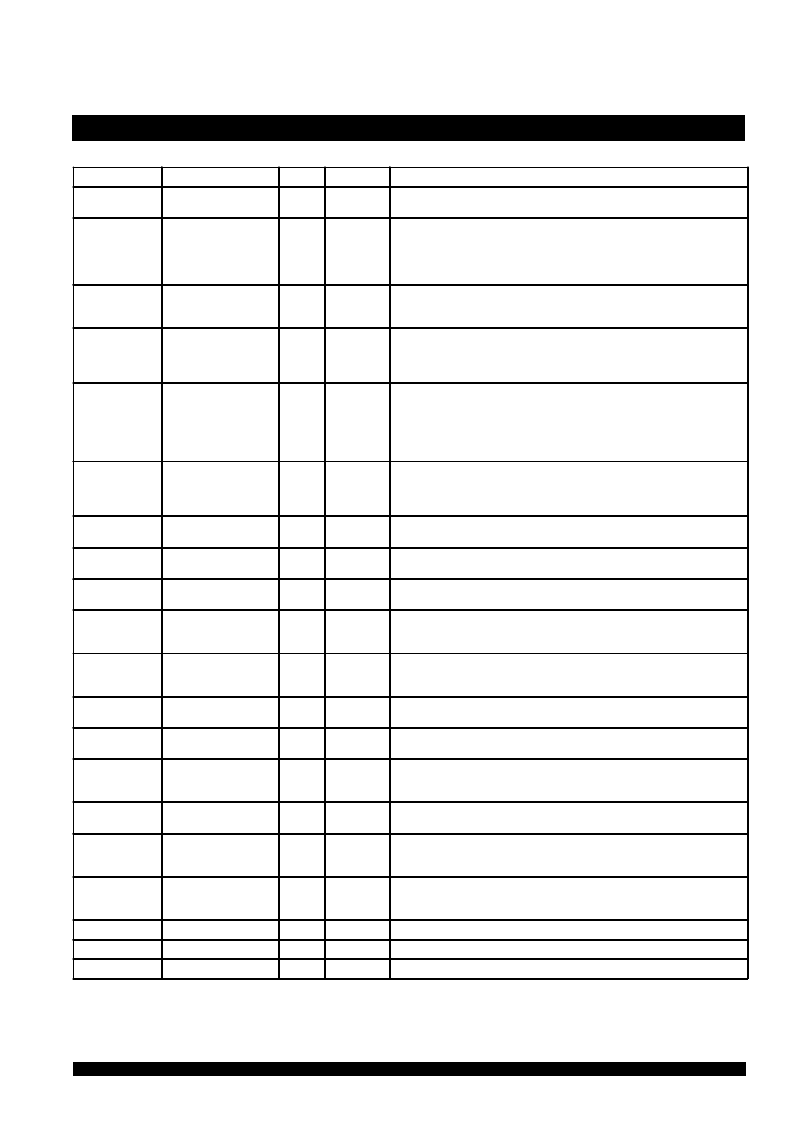
Pin Definition
(1)
Symbol
Pin Function
I/O
Active
NOTE:
1. All synchronous inputs must meet specified setup and hold times with respect to CLK.
Description
A
0
-A
17
Address Inputs
I
N/A
Synchronous Address inputs. The address register is triggered by a combination of the rising
edge of CLK, ADV/
LD
low
CEN
low and true chip enables.
ADV/
LD
Advance / Load
I
N/A
ADV/
LD
is a synchronous input that is used to load the internal registers wth newaddress and
control when it is sampled lowat the rising edge of clock with the chip selected. When
ADV/
LD
is low wth the chip deselected, any burst in progress is termnated. When ADV/
LD
is
sampled high then the internal burst counter is advanced for any burst that was in progress.
The external addresses are ignored when ADV/
LD
is sampled high.
R/
W
Read / Write
I
N/A
R/
W
signal is a synchronous input that identifies whether the current load cycle initiated is a
Read or Write access to the memory array. The data bus activity for the current cycle takes
place two clock cycles later
CEN
Clock Enable
I
LOW
Synchronous Clock Enable Input. When
CEN
is sampled high, all other synchronous inputs,
including clock are ignored and outputs remain unchanged. The effect of
CEN
sampled high
on the device outputs is as if the low to high clock transition did not occur For normal
operation,
CEN
must be sampled low at rising edge of clock.
BW
1
-
BW
4
Individual Byte
Write Enables
I
LOW
Synchronous byte write enables. Each 9-bit byte has its own active low byte write enable. On
load write cycles (When R/
W
and ADV/
LD
are sampled low) the appropriate byte write signal
(
BW
1
-
BW
4
) must be valid. The byte write signal must also be valid on each cycle of a burst
write. Byte Write signals are ignored when R/
W
is sampled high. The appropriate byte(s) of
data are written into the device two cycles later
BW
1
-
BW
4
can all be tied low if always doing
write to the entire 36-bit word.
CE
1
,
CE
2
Chip Enables
I
LOW
Synchronous active low chip enable.
CE
1
and
CE
2
are used with CE
2
to enable the
IDT71V3548. (
CE
1
or
CE
2
sampled high or CE
2
sampled low) and ADV/
LD
low at the rising
edge of clock, initiates a deselect cycle. The ZBT
TM
has a two cycle deselect, i.e., the data
bus wll tri-state two clock cycles after deselect is initiated.
CE
2
Chip Enable
I
HIGH
Synchronous active high chip enable. CE
2
is used with
CE
1
and
CE
2
to enable the chip. CE
2
has inverted polarity but otherwse identical to
CE
1
and
CE
2
.
CLK
Clock
I
N/A
This is the clock input to the IDT71V3548. Except for
OE
, all timng references for the device
are made wth respect to the rising edge of CLK.
I/O
0
-I/O
31
I/O
P1
-I/O
P4
Data Input/Output
I/O
N/A
Synchronous data input/output (I/O) pins. Both the data input path and data output path are
registered and triggered by the rising edge of CLK.
LBO
Linear Burst Order
I
LOW
Burst order selection input. When
LBO
is high the Interleaved burst sequence is selected.
When
LBO
is low the Linear burst sequence is selected.
LBO
is a static input and it must not
change during device operation.
OE
Output Enable
I
LOW
Asynchronous output enable.
OE
must be low to read data fromthe 71V3548. When
OE
is
high the I/O pins are in a high-impedance state.
OE
does not need to be actively controlled
for read and write cycles. In normal operation,
OE
can be tied low
TMS
Test Mode Select
I
N/A
Gives input command for TAP controller Sampled on rising edge of TDK. This pin has an
internal pullup.
TDI
Test Data Input
I
N/A
Serial input of registers placed between TDI and TDO. Sampled on rising edge of TCK. This
pin has an internal pullup.
TCK
Test Clock
I
N/A
Clock input of TAP controller Each TAP event is clocked. Test inputs are captured on rising
edge of TCK, while test outputs are driven fromthe falling edge of TCK. This pin has an
internal pullup.
TDO
Test Data Output
O
N/A
Serial output of registers placed between TDI and TDO. This output is active depending on the
state of the TAP controller
TRST
JTAG Reset
(Optional)
I
LOW
Optional Asynchronous JTAG reset. Can be used to reset the TAP controller but not required.
JTAG reset occurs automatically at power up and also resets using TMS and TCK per IEEE
1149.1. If not used
TRST
can be left floating. This pin has an internal pullup.
ZZ
Sleep Mode
I
HIGH
Synchronous sleep mode input. ZZ HIGH will gate the CLK internally and power down the
IDT71V3548 to its lowest power consumption level. Data retention is guaranteed in Sleep
Mode. This pin has an internal pulldown
V
DD
Power Supply
N/A
N/A
3.3V core power supply.
V
DDQ
Power Supply
N/A
N/A
3.3V I/O Supply.
V
SS
Ground
N/A
N/A
Ground.
5296 tbl 02
相關(guān)PDF資料 |
PDF描述 |
|---|---|
| IDT71V3548SA | 256K x 18 3.3V Synchronous ZBT SRAM 3.3V I/O, Burst Counter Pipelined Outputs |
| IDT71V3548SA100BG | 256K x 18 3.3V Synchronous ZBT SRAM 3.3V I/O, Burst Counter Pipelined Outputs |
| IDT71V3548SA100BGI | 256K x 18 3.3V Synchronous ZBT SRAM 3.3V I/O, Burst Counter Pipelined Outputs |
| IDT71V3548SA100BQ | 256K x 18 3.3V Synchronous ZBT SRAM 3.3V I/O, Burst Counter Pipelined Outputs |
| IDT71V3548SA100BQI | 256K x 18 3.3V Synchronous ZBT SRAM 3.3V I/O, Burst Counter Pipelined Outputs |
相關(guān)代理商/技術(shù)參數(shù) |
參數(shù)描述 |
|---|---|
| IDT71V3556S100BG | 功能描述:IC SRAM 4MBIT 100MHZ 119BGA RoHS:否 類別:集成電路 (IC) >> 存儲器 系列:- 產(chǎn)品變化通告:Product Discontinuation 05/Nov/2008 標(biāo)準(zhǔn)包裝:84 系列:- 格式 - 存儲器:RAM 存儲器類型:SRAM - 同步 ZBT 存儲容量:4.5M(128K x 36) 速度:75ns 接口:并聯(lián) 電源電壓:3.135 V ~ 3.465 V 工作溫度:-40°C ~ 85°C 封裝/外殼:119-BGA 供應(yīng)商設(shè)備封裝:119-PBGA(14x22) 包裝:托盤 其它名稱:71V3557SA75BGI |
| IDT71V3556S100BG8 | 功能描述:IC SRAM 4MBIT 100MHZ 119BGA RoHS:否 類別:集成電路 (IC) >> 存儲器 系列:- 產(chǎn)品變化通告:Product Discontinuation 05/Nov/2008 標(biāo)準(zhǔn)包裝:84 系列:- 格式 - 存儲器:RAM 存儲器類型:SRAM - 同步 ZBT 存儲容量:4.5M(128K x 36) 速度:75ns 接口:并聯(lián) 電源電壓:3.135 V ~ 3.465 V 工作溫度:-40°C ~ 85°C 封裝/外殼:119-BGA 供應(yīng)商設(shè)備封裝:119-PBGA(14x22) 包裝:托盤 其它名稱:71V3557SA75BGI |
| IDT71V3556S100BGI | 功能描述:IC SRAM 4MBIT 100MHZ 119BGA RoHS:否 類別:集成電路 (IC) >> 存儲器 系列:- 產(chǎn)品變化通告:Product Discontinuation 05/Nov/2008 標(biāo)準(zhǔn)包裝:84 系列:- 格式 - 存儲器:RAM 存儲器類型:SRAM - 同步 ZBT 存儲容量:4.5M(128K x 36) 速度:75ns 接口:并聯(lián) 電源電壓:3.135 V ~ 3.465 V 工作溫度:-40°C ~ 85°C 封裝/外殼:119-BGA 供應(yīng)商設(shè)備封裝:119-PBGA(14x22) 包裝:托盤 其它名稱:71V3557SA75BGI |
| IDT71V3556S100BGI8 | 功能描述:IC SRAM 4MBIT 100MHZ 119BGA RoHS:否 類別:集成電路 (IC) >> 存儲器 系列:- 產(chǎn)品變化通告:Product Discontinuation 05/Nov/2008 標(biāo)準(zhǔn)包裝:84 系列:- 格式 - 存儲器:RAM 存儲器類型:SRAM - 同步 ZBT 存儲容量:4.5M(128K x 36) 速度:75ns 接口:并聯(lián) 電源電壓:3.135 V ~ 3.465 V 工作溫度:-40°C ~ 85°C 封裝/外殼:119-BGA 供應(yīng)商設(shè)備封裝:119-PBGA(14x22) 包裝:托盤 其它名稱:71V3557SA75BGI |
| IDT71V3556S100BQ | 功能描述:IC SRAM 4MBIT 100MHZ 165FBGA RoHS:否 類別:集成電路 (IC) >> 存儲器 系列:- 產(chǎn)品變化通告:Product Discontinuation 05/Nov/2008 標(biāo)準(zhǔn)包裝:84 系列:- 格式 - 存儲器:RAM 存儲器類型:SRAM - 同步 ZBT 存儲容量:4.5M(128K x 36) 速度:75ns 接口:并聯(lián) 電源電壓:3.135 V ~ 3.465 V 工作溫度:-40°C ~ 85°C 封裝/外殼:119-BGA 供應(yīng)商設(shè)備封裝:119-PBGA(14x22) 包裝:托盤 其它名稱:71V3557SA75BGI |
發(fā)布緊急采購,3分鐘左右您將得到回復(fù)。